At JHYPCB, we specialize in producing high-quality PCBs for companies across various industries. As a leading PCB manufacturer in China, we leverage decades of experience and the latest technologies to deliver exceptional PCBs for all needs.
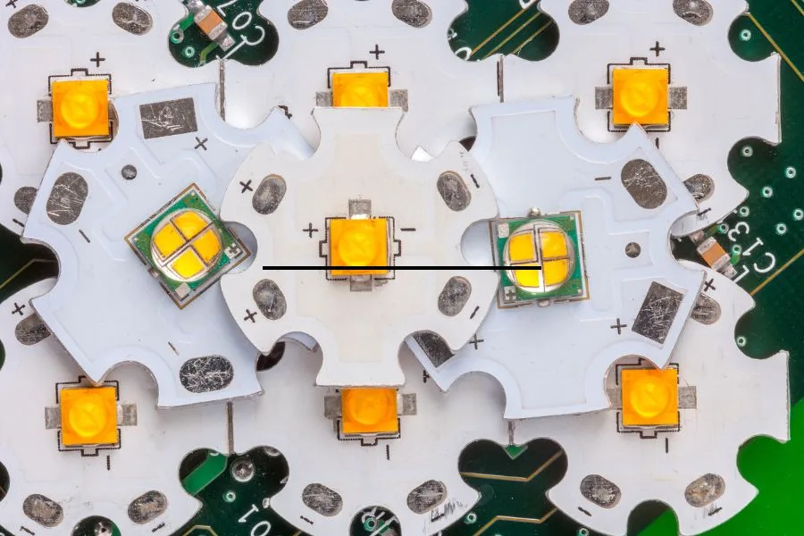
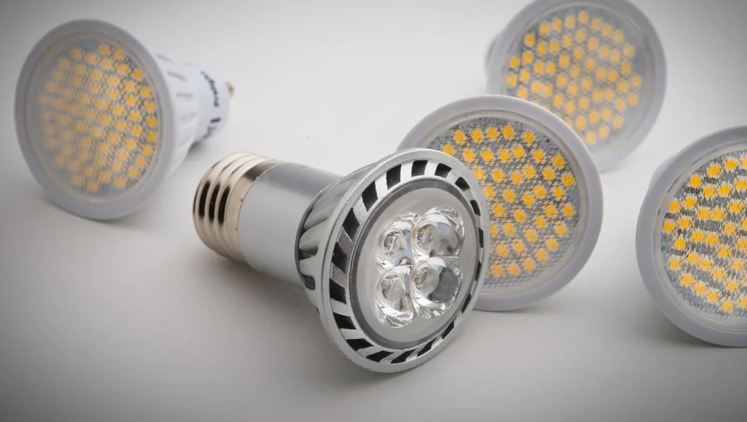
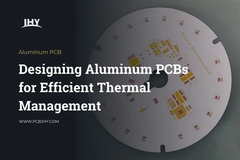
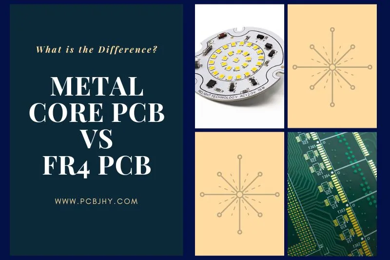
In recent years, we’ve seen growing demand for aluminum PCBs, which provide several benefits over traditional FR4 PCBs. Aluminum PCBs are lightweight, highly conductive, and withstand high temperatures – ideal for aerospace, automotive, LED, and other applications.
This comprehensive guide will walk through the aluminum PCB manufacturing process step-by-step. We’ll cover single-layer, double-layer, and multilayer aluminum PCB fabrication. By the end, you’ll understand the complete process our engineers use to create these specialized PCBs.
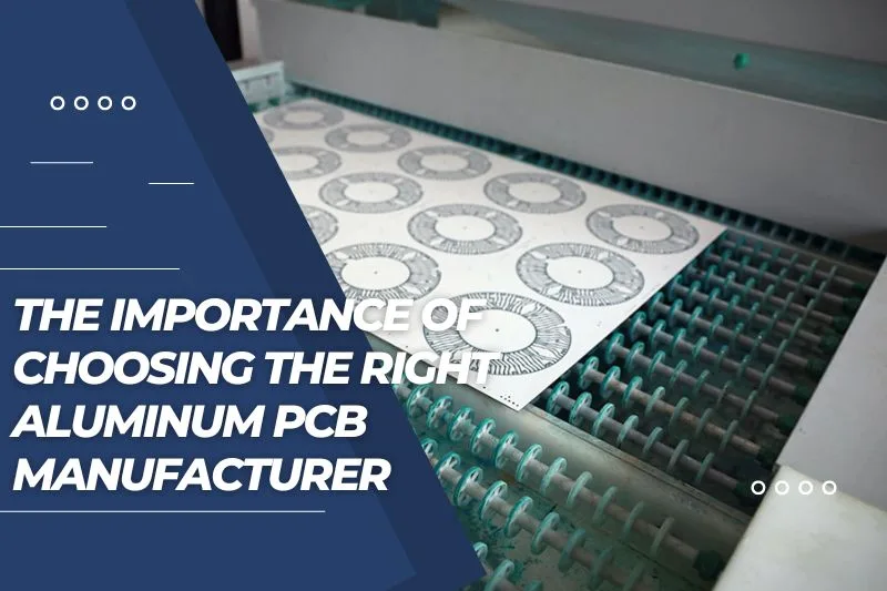
With in-depth expertise in aluminum PCB manufacturing, JHYPCB produces all types of these PCBs at our factory in China. We follow rigorous quality control and inspection at every step. Our optimized fabrication techniques enable high yields, quick turnaround times, and consistently flawless aluminum PCBs.
We’re excited to share the details of our aluminum PCB manufacturing process with you. Please don’t hesitate to contact JHYPCB to discuss your specific aluminum PCB requirements. Our engineers are ready to help bring your project from concept to high-quality realization.

Single-Sided Aluminum PCB Manufacturing Process
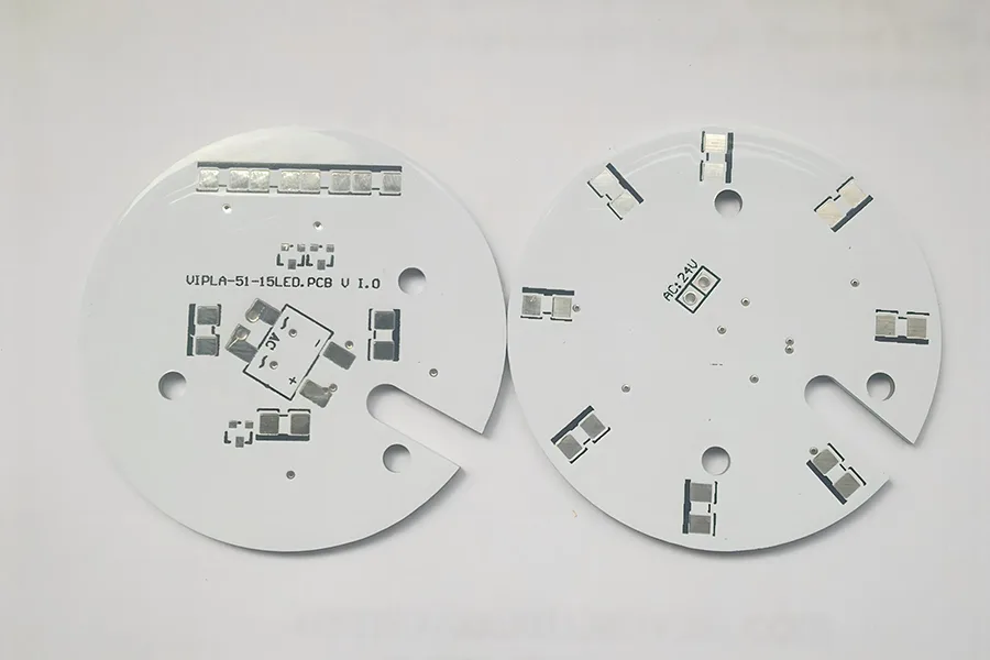
Single-layer aluminum PCB is a printed circuit board consisting of a single layer of conductive material (usually copper) on an aluminum substrate. The aluminum substrate provides excellent thermal conductivity and dissipates heat quickly, making it a popular choice for applications that require high power or generate a lot of heat.
Learn more about our single-layer PCB manufacturing service
Single-layer aluminum PCBs are typically used in electronic devices such as LED lighting, power supplies, motor controllers, and automotive electronics. They are also commonly used in the aerospace industry due to their ability to withstand high temperatures and harsh environmental conditions.
The manufacturing process for single-layer aluminum PCBs is similar to that of traditional PCBs, with some differences in the materials used and the etching process. The aluminum substrate is coated with a layer of copper, which is then etched to create the desired circuit pattern. The resulting PCB is lightweight, durable, and able to dissipate heat efficiently, making it an ideal choice for many applications.
The single-layer aluminum PCB manufacturing process typically involves the following steps:
Step I. Board Preparation
- Cut the aluminum sheet to the desired size
- Clean the surface with a suitable solvent to remove any dirt or grease
- Apply a layer of etch resist to the surface of the aluminum sheet
- Place a layer of dry film photoresist onto the etch-resist layer
- Expose the photoresist layer to UV light through a mask to transfer the desired pattern onto the surface of the aluminum sheet.
- Develop the photoresist layer to remove unexposed areas, leaving behind the desired pattern.
Step II. Etching
- Immerse the aluminum sheet into an etching solution, such as ferric chloride or ammonium persulfate.
- The etchant solution will dissolve the exposed areas of aluminum not covered by the photoresist layer, leaving behind the desired circuit pattern.
- Rinse the board with water to remove any etchant residue
- Remove the photoresist layer using a suitable solvent
Step III. Drilling
- Drill holes for component leads or through-hole plating
- Deburr the drilled holes using a deburring tool
Step IV. Plating
- Apply a layer of copper to the circuitry and plate through-holes using an electroplating process.
- Apply a layer of solder mask to protect the copper traces
- Cure the solder mask using UV light
Step V. Finishing
- Apply a layer of silkscreen or legend to label component placements
- Apply a layer of surface finish, such as OSP (Organic Solderability Preservative) or ENIG (Electroless Nickel Immersion Gold), to protect the exposed copper traces and pads from oxidation
Step VI. Testing
- Test the completed PCB for functionality and continuity using a suitable testing method, such as a flying probe or bed of nails tester.
Step VII. Final Inspection and Packaging
- Inspect the completed PCB for any defects or issues
- Package the PCB in a suitable anti-static bag for protection during transportation and storage
Aluminum PCB Manufacturer and Manufacturing Process
Double Sided Aluminum PCB Manufacturing Process
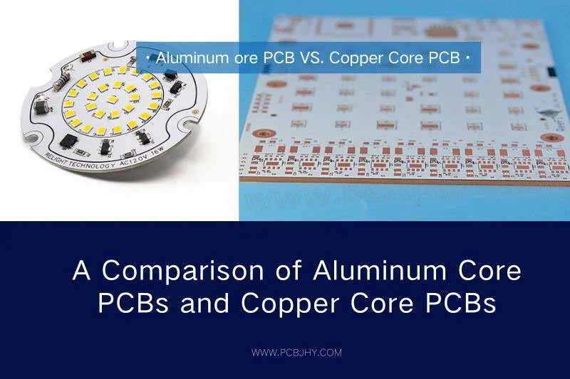
Double-sided aluminum PCBs are a type of PCB that has a metal core made of aluminum, with circuitry on both the top and bottom sides of the board. Unlike single-sided aluminum PCBs, which have circuitry on only one side, double-sided aluminum PCBs can support more complex electronic designs and accommodate more components. Double-sided aluminum PCBs are commonly used in high-power and high-temperature applications, such as power electronics, LED lighting, and automotive applications, where their superior thermal conductivity and heat dissipation properties make them an ideal choice. The manufacturing process for double-sided aluminum PCBs is more complex than that of single-sided aluminum PCBs, but the resulting board is more versatile and capable of supporting a wider range of electronic designs.
Learn more about our double-sided PCB manufacturing service
The double-sided aluminum PCB manufacturing process typically involves the following steps:
Step I. Board Preparation
- Cut the aluminum sheet to the desired size
- Clean the surface with a suitable solvent to remove any dirt or grease
- Apply a layer of etch resist to the surface of the aluminum sheet
- Place a layer of dry film photoresist onto the etch-resist layer
- Expose the photoresist layer to UV light through a mask to transfer the desired pattern onto the surface of the aluminum sheet.
- Develop the photoresist layer to remove unexposed areas, leaving behind the desired pattern.
Step II. Etching
- Immerse the aluminum sheet into an etching solution, such as ferric chloride or ammonium persulfate.
- The etchant solution will dissolve the exposed areas of aluminum not covered by the photoresist layer, leaving behind the desired circuit pattern on one side of the aluminum sheet.
- Rinse the board with water to remove any etchant residue
- Remove the photoresist layer using a suitable solvent
- Repeat the above steps to create a second circuit pattern on the other side of the aluminum sheet
Step III. Drilling
- Drill holes for component leads or through-hole plating
- Deburr the drilled holes using a deburring tool
Step IV. Plating
- Apply a layer of copper to the circuitry and plated through-holes using an electroplating process.
- Apply a layer of solder mask to protect the copper traces on both sides of the board.
- Cure the solder mask using UV light
Step V. Finishing
- Apply a layer of silkscreen or legend to label component placements
- Apply a layer of surface finish, such as OSP (Organic Solderability Preservative) or ENIG (Electroless Nickel Immersion Gold), to protect the exposed copper traces and pads from oxidation
Step VI. Testing
- Test the completed PCB for functionality and continuity using a suitable testing method, such as a flying probe or bed of nails tester.
Step VII. Final Inspection and Packaging
- Inspect the completed PCB for any defects or issues
- Package the PCB in a suitable anti-static bag for protection during transportation and storage

Multi-Layer Aluminum PCB Manufacturing Process
Multi-layer aluminum PCBs are printed circuit boards with multiple layers of conductive material separated by layers of insulating material, with a metal core made of aluminum. The manufacturing process for multi-layer aluminum PCBs is more complex than that of single-sided or double-sided aluminum PCBs, as it involves laminating several layers of copper and insulating material onto the aluminum core.
The multi-layer aluminum PCB manufacturing process typically involves the following steps:
Step I. Board Preparation
- Cut aluminum sheets to the desired size
- Clean the surfaces of the aluminum sheets with a suitable solvent to remove any dirt or grease.
- Apply a layer of etch resist to both sides of the aluminum sheets
- Apply a layer of dry film photoresist onto the etch-resist layer
- Expose the photoresist layer to UV light through a mask to transfer the desired pattern onto the surface of the aluminum sheet
- Develop the photoresist layer to remove unexposed areas, leaving behind the desired pattern
- Repeat the above steps to create the desired number of layers
Step II. Lamination
- Align and stack the layers on top of each other using a lamination press
- Apply heat and pressure to bond the layers together into a single multilayer board
- The heat and pressure also activate the adhesive layer in the prepreg, which bonds the layers together
Step III. Drilling
- Drill holes for component leads or through-hole plating
- Deburr the drilled holes using a deburring tool
Step IV. Plating
- Apply a layer of copper to the circuitry and plate through-holes using an electroplating process.
- Repeat the plating process for each layer of the board
- Apply a layer of solder mask to protect the copper traces on both sides of the board
- Cure the solder mask using UV light
Step V. Finishing
- Apply a layer of silkscreen or legend to label component placements
- Apply a layer of surface finish, such as OSP (Organic Solderability Preservative) or ENIG (Electroless Nickel Immersion Gold) to protect the exposed copper traces and pads from oxidation
Step VI. Testing
- Test the completed PCB for functionality and continuity using a suitable testing method, such as a flying probe or bed of nails tester.
Step VII. Final Inspection and Packaging
- Inspect the completed PCB for any defects or issues
- Package the PCB in a suitable anti-static bag for protection during transportation and storage

Comparison with Traditional PCB Manufacturing Processes
I. Material Properties
- Aluminum PCBs have superior thermal conductivity and heat dissipation compared to traditional PCBs, which makes them more suitable for high-power and high-temperature applications.
- Traditional PCBs are typically made of fiberglass or plastic materials that do not have the same thermal properties as aluminum PCBs
- Aluminum PCBs are also more durable and resistant to environmental factors such as humidity and temperature changes.
II. Manufacturing Processes
- The manufacturing process for aluminum PCBs involves the use of an etch resist, photoresist, and a lamination press, while traditional PCBs use a combination of etching, drilling, and plating processes.
- Aluminum PCBs can be manufactured using a single-sided, double-sided, or multi-layer process, while traditional PCBs are typically limited to single or double-sided designs.
- The etching process used in traditional PCB manufacturing can produce waste materials that are harmful to the environment if not disposed of properly, while aluminum PCB manufacturing produces less waste and is more environmentally friendly.
III. Cost
- Aluminum PCBs are generally more expensive to manufacture than traditional PCBs due to the higher cost of materials and the more complex manufacturing process.
- However, the increased thermal conductivity and durability of aluminum PCBs can reduce the need for additional heat sinks or cooling systems, which can ultimately result in cost savings in the long run.
IV. Applications
- Aluminum PCBs are commonly used in high-power and high-temperature applications such as power electronics, LED lighting, and aerospace, where traditional PCBs may not be able to withstand the heat generated.
- Traditional PCBs are still widely used in a variety of applications, including consumer electronics, medical devices, and automotive applications.
Overall, aluminum PCBs may be more expensive to manufacture than traditional ones, but their superior thermal conductivity and durability make them ideal for certain high-power and high-temperature applications. However, traditional PCBs are still a popular choice for a wide range of applications and offer a more cost-effective option for designs that do not require the same level of thermal performance.
Conclusion
We hope this guide gave you an in-depth look into the aluminum PCB fabrication process. As you can see, producing high-quality aluminum PCBs requires expertise, precision, and stringent quality control at every step.
At JHYPCB, we’ve optimized each aspect of the manufacturing process to deliver exceptional single layer, double layer, and multilayer aluminum PCBs. Our skilled engineering team leverages the latest cutting-edge equipment to fabricate aluminum PCBs for customers worldwide.
With robust capabilities and decades of experience, JHYPCB is your reliable partner for all aluminum PCB requirements. Whether you need rapid prototyping or high-volume production, we have the technical knowledge and manufacturing capabilities to fulfill your needs.
Ready to get started on your aluminum PCB project? Contact our engineers today to discuss your requirements. We’re committed to working as an extension of your team to take your product from concept to finished boards. With JHYPCB as your trusted aluminum PCB supplier, you can leverage our expertise to make your project a success.
If you are looking for high-quality aluminum PCB manufacturing services, look no further than us! As a professional aluminum PCB manufacturer, we specialize in providing top-notch manufacturing services for single-sided, double-sided, multi-layer, hybrid, and flexible aluminum PCBs. Our state-of-the-art facilities and experienced team of experts ensure that all of our products are of the highest quality and meet the strictest industry standards. Whether you are working on a high-power LED lighting project or a complex aerospace application, we have the expertise and capabilities to deliver the aluminum PCBs you need. Contact us today to learn more about our services and how we can help you with your next project!
Related Reading