


Your Trusted Prototype PCB Manufacturing And Assembly Partner.
When you partner with us, we do everything to ensure your PCB manufacturing and assembly are completed on time to your specifications with the highest quality.
Leading manufacturer of PCB Fabrication and Assembly in China.
Printed Circuit Boards are the cornerstone of modern electronics design, providing a reliable and efficient method for connecting electronic components. With the constant drive towards miniaturization and enhanced functionality, designers are always looking for ways to pack more power into smaller spaces. That’s where PCB microvias come in. Microvias are tiny holes drilled into a PCB that allows for the creation of more complex and compact designs. In this article, we will explore the basics of PCB microvias, their different types, and their benefits over traditional circuit board designs. We will also go over the implementation process and design considerations for microvias, as well as the cost implications. By the end of this article, you will have a comprehensive understanding of what microvias are, how they work, and whether they could be beneficial for your next PCB design project.
According to the new definition as defined in IPC-T-50M, a microvia is a blind structure with a maximum aspect ratio of 1:1 that terminates on a target land with a total depth of no more than 0.25mm, measured from the structure’s capture land foil to the target land. Microvias have a smaller diameter than traditional vias, which allows for greater packing density of components on a PCB. In fact, PCB companies typically classify vias with a diameter of less than 150 microns as microvias. This feature is especially important for high-speed circuits, as microvias have a lower parasitic capacitance compared to traditional vias.
Microvias are also known as micro vias, micro-via, μVia, laser via, or laser ablated via. The manufacturing process for microvias can be more complex and expensive than for traditional vias, as they are drilled using lasers instead of mechanical drilling. However, laser drilling significantly reduces the likelihood of manufacturing defects. Microvias are used to connect one layer of a PCB to its adjacent layer and are commonly found in high-density interconnect (HDI) substrates and PCBs to accommodate the high input/output (I/O) density of advanced packages.
Driven by the demand for portability and wireless communications, the electronics industry aims to produce affordable, light, and reliable products with increased functionality. At the electronic component level, this translates to components with increased I/Os and smaller footprint areas, while at the printed circuit board and package substrate level, HDIs with finer traces and spaces and smaller vias are used. Microvias are a crucial element in achieving these goals, as they enable denser PCBs with more complex designs.
Structural definition of microvias in IPC-6012.
As electronics products become increasingly complex, we face the challenge of miniaturization for both the product itself and its circuit board. With smaller components and features, combined with limited board space, we require finer track and gap and more interconnections for higher circuit board densities.
This demand results in an increasing number of holes with smaller diameters, surpassing the density limits of traditional plated through holes. This is where microvias come into play – laser-drilled holes that are smaller in diameter than mechanically drilled holes and only connect certain layers (such as layers 1-2) instead of passing through and connecting all layers.
Microvias enable us to increase the component density on a PCB, reduce parasitic capacitance, and allow for better signal integrity. They also enable us to create thicker laminates for increased reliability and facilitate the integration of passive components directly into the circuit board, leading to greater design flexibility and overall product performance.
Therefore, the use of microvias is becoming more and more widespread in modern electronics, particularly in applications such as HDI circuit boards and mobile devices. As these technologies continue to advance, we can expect microvias to play an increasingly critical role in the future of electronics manufacturing.
Microvias offer a range of benefits for PCB design and manufacture. These include:
The use of microvias enables designers to achieve higher density interconnects, allowing for more circuitry per unit of board area. This can be particularly advantageous in designs where space is at a premium.
Microvias have lower inductance and capacitance than traditional through-hole vias, resulting in improved signal integrity. This can be particularly important in high-speed designs where signal quality is critical for overall system performance.
The smaller size of microvias can help to improve thermal management, as they permit heat to be dissipated more efficiently. This is particularly important in designs where components generate significant amounts of heat, or where thermal management is critical to product performance.
The use of microvias can help to reduce the size and weight of PCBs, making them particularly attractive for portable and handheld devices. This is achieved by reducing the overall board area required for interconnects, as well as by reducing the volume of material required for the vias themselves.
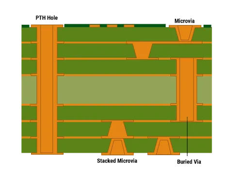
Staggered Microvias: These are the most commonly used microvias. Staggered microvias are drilled on both sides of the PCB and have an offset from each other. This allows for higher component density and smaller via diameters.
Stacked Microvias: Stacked microvias are created by drilling multiple layers of the PCB at the same location, creating a connection between the layers. These microvias save space and improve the signal quality by reducing parasitic capacitance.
Skipped Microvias: Microvias formed in one operation, penetrating two or more HDI dielectric layers and terminating at one or more different layers.

| Microvias | Staggered | Stacked | Skipped |
|---|---|---|---|
| Outer Layer Surface |
+++ smallest surface |
+ largest surface |
++ medium surface |
| Copper Barrel Stability |
+++ shortest connection |
++ connection to copper layer |
+ largest connection |
| Plating Surface |
+++ largest |
+ smallest |
++ medium |
| Lasting Time |
— 2x lasting 2x registering |
— 2x lasting 1x registering |
– 1x lasting 1x registering |
| Press Cycles |
— 2 |
+ 1 |
+ 1 |
| Costs | — | — | — |
PCB microvia holes can be filled with resin and then ground to obtain a flat surface, ensuring the planarity of the subsequent layer. Resin filling can be used individually for buried microvias, or together with copper plating (cap) for blind microvias. The thickness of copper plating for through holes, blind vias, buried vias, blind and buried microvias, and buried via cores can be found in the latest IPC-6012D. Additionally, the copper cap plating thickness for filled holes can also be found in this standard.
| Copper Plating Thickness | Class 2 | Class 3 | Class 3A* | |
|---|---|---|---|---|
| Through, Blind, Buried Vias (>2Layers) (Min) | Wrap: | 20μm [0.79mil] | 25μm [0.98mil] | 25μm [0.98mil] |
| Thin Areas: | 18μm [0.71mil] | 20μm [0.79mil] | 20μm [0.79mil] | |
| Wrap: | 5μm [0.20mil] | 12μm [0.47mil] | 12μm [0.47mil] | |
| Through, Blind, Buried μVias (>2Layers) (Min) | Wrap: | 12μm [0.47mil] | 12μm [0.47mil] | 20μm [0.79mil] |
| Thin Areas: | 10μm [0.39mil] | 10μm [0.39mil] | 18μm [0.71mil] | |
| Wrap: | 5μm [0.20mil] | 6μm [0.24mil] | 6μm [0.24mil] | |
| Buried Vias Core (2Layers) (Min) | Average: | 15μm [0.59mil] | 15μm [0.59mil] | 20μm [0.79mil] |
| Thin Areas: | 13μm [0.51mil] | 13μm [0.51mil] | 18μm [0.71mil] | |
| Wrap: | 5μm [0.19mil] | 7μm [0.27mil] | 7μm [0.27mil] | |
| Cap Plating of Filled Holes | Min: | 5μm [0.19mil] | 12μm [4.7mil] |
76μm [3mil]-General 50μm [2mil]-BGA |
| Max: | 127μm [5mil] | 76μm [3mil] | 50μm [2mil] | |
The IPC-2226 specifies the HDI structures by type, with three types highlighted in the accompanying images.
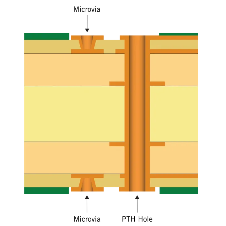
This structure features a single layer of microvias on one or both sides of the core and utilizes both microvias and through holes for interconnection. Maintaining a ratio of 0.8:1 is crucial for the microvia. Additionally, this structure solely utilizes blind holes and does not employ passage to buried holes.
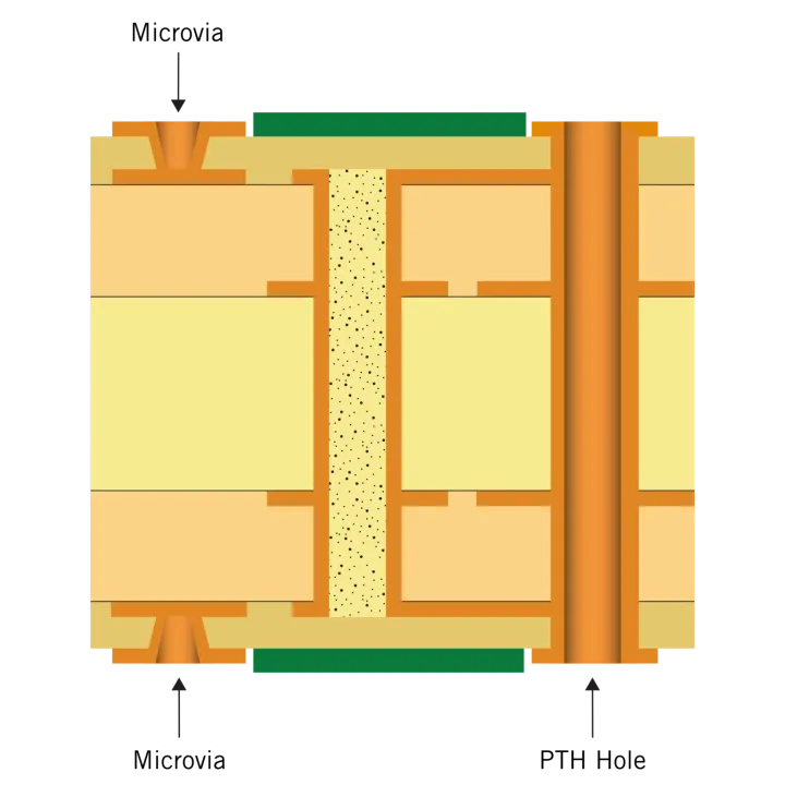
These structures are comparable to type 1 as they also feature only a single layer of microvia on one or both sides of the core and utilize both microvias and through holes for interconnection. However, in contrast to type 1, these structures also incorporate buried holes.
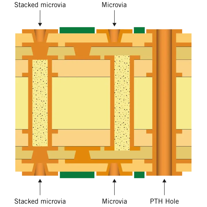
The PCB High Density Interconnect (HDI) boards with at least two layers of microvias on one or both sides of the core are the most intricate and difficult ones for factories to produce. Type 2 HDI boards, on the other hand, use through-holes in addition to blind and buried vias.
Smaller micro-vias and higher quality standards in the formation process are increasingly necessary for reliable interconnections between sequential layers of HDI boards. While mechanical drilling is a well-known method in the PCB industry, it has limitations in throughput, efficiency, and accuracy, particularly with glass-fiber reinforced materials. Thus, it is unsurprising that laser ablation has quickly emerged as the leading method for microvia formation due to its flexibility and versatility.
Mechanical drilling is a widely used technology to create microvias in printed circuit boards. In this technique, a drill bit is mechanically rotated with high speed and pressure against the PCB surface to create small holes with diameters ranging from 75 to 150 microns. The drill is typically made of carbide or high-speed steel and is cooled with water or compressed air to reduce heat buildup and prevent damage to the drill bit.
Mechanical drilling is a cost-effective and reliable method of creating microvias, especially for low-volume PCB production. However, it has some limitations, such as its ability to create only simple hole geometries, its tendency to create burrs and rough surfaces, and the need for frequent drill bit replacements.
To overcome these limitations, other technologies such as CO2 and UV laser drilling have been developed for precise microvia manufacturing.
CO₂ lasers emit infrared (IR) light in a wavelength range of 9.4μm to 10.6μm. They are commonly used for drilling substrates such as resin epoxy, fiberglass, PP, PI, PET, adhesive, and coverlay, as they cannot cut through copper. CO₂ lasers are available in a wide range of output power, making them ideal for fast drill processing in circuit board substrates. However, their relatively long wavelength limits the minimum focus diameter in a given working field area. This means that the creation of vias with diameters smaller than 3mil (0.075mm) is at the physical limits of this technology.
The solid-state laser used for microvia formation is another type of laser that emits ultraviolet (UV) light, usually Nd-YAG. The absorption spectra of copper, epoxy, polyimide, and glass show that UV light with a wavelength of 355nm (0.355μm) is absorbed by all these materials. Additionally, UV light is emitted in short high-power pulses. By focusing it precisely to a small spot, the extreme high-power density creates very concentrated plasma, allowing pinpoint ablation of the material.
Using UV laser technology for drilling printed circuit boards offers several advantages. It is possible to drill both copper and substrate (including coverlay and EMI shielding film) using only one equipment, without the need for photochemical etching of the outer copper layer. UV lasers can also remove the copper layer to expose the fiducials for proper alignment between drill pattern and artwork of the inner layers. Microvias with superior quality, large and clean bottoms that are textured and won’t require desmearing can be produced.
The exposure of energy in a very small spot for a very short time limits heat spread-out to the drill hole’s environment. This, in turn, reduces the danger of delamination of mushroom-shaped holes. UV lasers also enable the production of “stacked vias” that connect three layers of the board with one another. Other benefits of UV laser formation of microvias are the excellent alignment to the inner layer circuitry by using fiducials on the inner layer, which allows the use of smaller land pads, and the capability to form stacked vias that connect three layers, reducing the steps involved in the sequential build-up (SBU) process.
HDI PCB manufacturers are capable of using various dielectrics for microvia boards, ranging from conventional glass reinforced epoxy to ultra-thin unreinforced materials like resin coated copper foil (RCC). The choice of dielectric type and thickness for the microvia layer depends on the product’s end-use environment, expected operating life, and necessary board-level attributes, such as dielectric withstand voltage and resin content to fill buried vias or avoid resin starvation. Before determining the microvia diameter, the PCB designer must first select the thickness and type of dielectric for the microvia layer and a suitable aspect ratio for blind microvias. The acceptable aspect ratio values depend on the PCB board supplier and indicative of their hole configuration forming and plating capabilities. Additionally, the outer copper foil thickness should be considered when designing microvias.
To calculate the required as-formed diameter of the microvia, use the following equation:
Microvia Diameter = (Dielectric Thickness on Outer Layer + Outer Copper Foil Thickness) / Aspect Ratio
The target pad and capture pad diameters are then determined by adding two annular ring widths and a fabrication allowance to the as-formed diameter of the microvia. The required microvia fabrication allowance is dependent on material behavior and fabrication process tolerances.
Therefore, the final formulas for the target pad diameter and capture pad diameter are as follows:
Target Pad Diameter = Microvia Diameter + 2 x Annular Ring Widths
Capture Pad Diameter = Microvia Diameter + 2 x Annular Ring Widths
A microvia is a small diameter drilled hole in a printed circuit board (PCB), typically less than 0.15mm in diameter.
Microvias are used to connect different layers of a PCB without adding additional layers or increasing the board thickness, which can save space and reduce overall PCB size.
A through-hole via goes all the way through the PCB while a microvia is a blind or buried via that only connects certain layers of the PCB.
Microvias allow for increased routing density, reduce signal distortion and are less likely to be affected by electromagnetic interference (EMI). They also reduce the number of layers required in a PCB design, leading to cost savings and improved reliability.
UV laser drilling and CO2 laser drilling are two common techniques used to create microvias.
UV laser drilling offers higher precision and accuracy in creating smaller microvias, making it ideal for high-density PCB designs. It also reduces the risk of thermal damage to the PCB.
CO₂ laser drilling can create larger microvias in a shorter amount of time, making it ideal for mid-density PCB designs. It is also capable of drilling through thicker materials and is more cost-effective than UV laser drilling.
Designers must consider the minimum annular ring size, drill bit size and aspect ratio (the ratio between hole diameter and board thickness) when designing microvias. They must also account for the fact that the hole is not completely through the board, so additional measures must be taken to ensure proper electrical connections between layers.
When you partner with us, we do everything to ensure your PCB manufacturing and assembly are completed on time to your specifications with the highest quality.
Fill out the form below, and we will get back to you within the next 24
hours to complete the order, and then you’re all set to get started!
Prefer to email? Feel free to contact us directly at sales@pcbjhy.com.