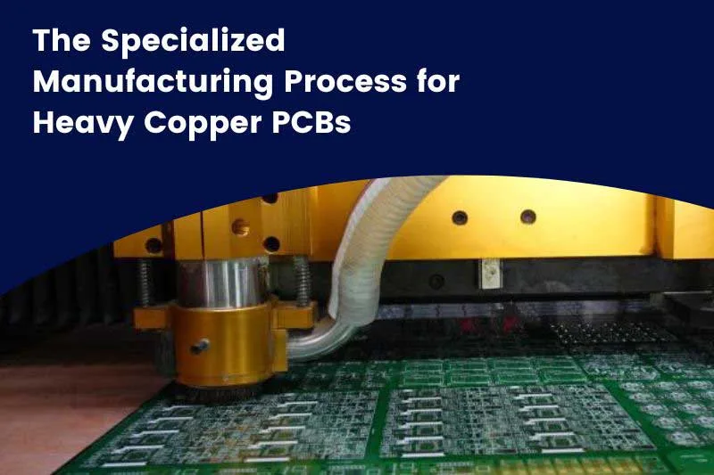
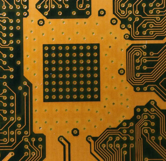
With the rise of electric vehicles, renewable energy, and other high-power applications, there has been increasing demand for heavy copper PCBs. Heavy copper PCBs utilize thicker copper layers, sometimes exceeding 3 or 6 oz. copper thickness, to handle higher current levels and power loads. The thick copper provides several benefits – it allows for better thermal management, reduces current density, and lowers power losses across the board. This makes heavy copper PCBs ideal for power electronics, motor controls, battery management systems, inverters, and other devices that must withstand high temperatures and current flows. However, the manufacturing process of heavy copper PCBs also poses unique challenges compared to standard PCBs. At JHYPCB, a leading PCB manufacturer in China, we leverage over 10 years of experience to deliver high-quality, reliable heavy copper PCB prototypes and mass production runs to customers worldwide. In this blog, we will outline the key steps, considerations, and controls involved in effectively fabricating heavy copper PCBs
Heavy Copper PCB Design Considerations
The design stage is crucial in ensuring the performance and reliability of heavy copper PCBs. Some key design factors must be accounted for:
- Copper Thickness – The most defining characteristic of a heavy copper board is its thicker copper layers, typically from 2 oz. to 6 oz. or even more. The copper thickness used depends on the required current carrying capacity and heat dissipation needs.
- Layer Count – Heavy copper PCBs tend to have higher layer counts to accommodate thicker copper and meet circuit routing needs. 4-12+ layers are common.
- Dielectric Materials – The separating insulating materials must have high thermal conductivity to transfer heat efficiently from the copper layers. Common materials include ceramic, FR-4, IMS, aluminum nitride, etc.
- Thermal Management – Thick copper itself helps dissipate heat, but thermal vias, cooling pads, and other provisions must be included for managing heat efficiently.
- Design Rules – Panelization, line spacing, hole sizes, etc. need to follow specified design rules to avoid fabrication issues.
Related Reading: How to Design a Heavy Copper PCB?

Heavy Copper PCB Manufacturing Process Step by Step
Fabricating heavy copper PCBs requires specialized processes at each stage to handle the thicker copper and high layer counts.
Inner Layer Processing – Direct imaging techniques create ultra-fine circuit patterns on the inner layers. A combination of printing and etching can build up very thick copper layers, along with high-aspect ratio plating processes.
Outer Layer Processing – The outer layers go through lithography, photoresist coating, imaging, and etching to form the tracks and pads. Additional pattern plating can further increase copper thickness. Automated optical inspection ensures minimal defects.
Layer Bonding – The inner and outer layers are precisely aligned and laminated using high temperature and pressure. The bonding process parameters are adjusted to accommodate the thick copper layers.
Via Formation – Small diameter vias are drilled through the PCB using specialized bits. The high-aspect ratio vias are then plated with copper to connect the layers electrically.
Testing and Inspection – Heavy copper PCBs undergo electrical testing, and automated optical and X-ray inspection at multiple stages to validate quality. This ensures reliability under thermal and mechanical stresses.
Finishing processes for heavy copper PCBs
Once the conductive copper layers and connections are fabricated, the heavy copper PCB moves through a set of finishing processes:
Solder Mask – A layer of epoxy-based solder mask is applied over the entire board surface, except the solder pads. This protects the copper from oxidation and prevents solder bridges.
Legend Printing – The component legends are printed on the solder mask for clear identification. This aids circuit assembly later.
Edge Profiling – The board outline is cut into shapes and the edges are profiled for smoothness. Corner chamfering prevents crack initiation.
Plating – Gold or tin layers are plated over the exposed solder pads and vias to facilitate soldering and protect against corrosion.
Testing – The finished board again undergoes electrical testing, AOI inspection, etc. to validate all functionality before shipment.
These finishing steps complete the heavy copper PCB fabrication. The thick boards are now ready for component assembly and installation, where they will serve in high-power, high-current applications ranging from electric vehicle drivetrains to renewable energy conversion systems.

Quality control and reliability testing for heavy copper PCBs
Robust quality control and reliability testing ensure the durability of heavy copper PCBs under demanding conditions.
Process Controls – Strict process controls are implemented at each fabrication stage, including parameters like plating thickness, lamination temperature/pressure, via dimensions, etc.
Inspection – In-process inspection and non-destructive testing methods like X-ray, AOI, flying probe, etc. validate quality.
Thermal Stress Tests – Boards are subjected to repeated thermal cycles, temperature shock, and long-duration heat soaks to ensure integrity under temperature extremes.
Mechanical Tests – Vibration, shock, and bend tests verify boards can withstand mechanical stresses during shipping, assembly, and service.
Electrical Tests – The board’s insulation resistance, continuity between tracks, dielectric withstand voltage, and other parameters are evaluated through electrical testing.
Analysis – Cross-section analysis of plated through holes, process audits, and failure mode analysis provide feedback to further improve manufacturing processes.
With these comprehensive quality practices, JHYPCB produces highly reliable, consistent heavy copper PCBs ready for the most demanding applications.
Heavy Copper PCB Manufacturing Process Notes and Tips
Specialized Manufacturing Process: The manufacture of heavy copper PCBs requires specialized processes and equipment. These processes include higher copper foil pressure and longer electrolyte deposition times to ensure a strong bond between the copper foil and the substrate.
- Multiple Copper Layers: Heavy copper PCBs often have multiple copper layers, with each layer requiring its own deposition process. This can increase the complexity and time required for manufacture.
- Thicker Substrates: Heavy copper PCBs require thicker substrates to support the weight of the copper layers. This can also affect the routing and drilling of the PCB.
- Controlled Impedance: Heavy copper PCBs often require controlled impedance for high-speed signal transmission. This requires precise control of the copper thickness and layer spacing.
Common Issues:
- Uneven Electrodeposition: Heavy copper PCBs require a longer electrodeposition time, which can result in uneven copper thickness across the board.
- Warping: The high copper weight can cause the board to warp during the manufacturing process, resulting in uneven board thickness and difficulties in assembly.
- Internal Connectivity: Heavy copper PCBs often require plated through-holes (PTHs) for internal connectivity. These PTHs can be difficult to manufacture and may result in reliability issues.
- Delamination: The increased weight and thickness of heavy copper PCBs can lead to delamination between the copper layers and substrate.
Conclusion
The manufacturing of heavy copper PCBs is undoubtedly more complex compared to standard PCBs. The thick copper layers and high layer counts require specialized fabrication processes, quality control measures, and reliability testing. Key factors like thermal management, mechanical robustness, and electrical performance have to be built into the board by design and manufacturing enhancements at each stage. At JHYPCB, we have invested in the technical expertise and precision manufacturing capabilities to deliver high-quality heavy copper PCB prototypes and production runs. With over a decade of experience, we understand the nuances of heavy copper PCB fabrication. We collaborate closely with customers right from the design stage to the finished board, to create custom heavy copper PCBs optimized for their specific application needs. With our rigorous quality standards, advanced production facilities, and veteran engineering support, customers can rely on JHYPCB as a trusted heavy copper PCB manufacturing partner.