Printed circuit boards are the foundation of electronics. They provide the mechanical structure to mount components and connect them together with conductive copper traces. While simple circuits can be built on 2-layer PCBs, more complex designs require multilayer boards with additional layers “stacked up” to provide more routing and functionality.
The sequence and choice of layers in a PCB stackup is an important design consideration that affects performance, manufacturability, and cost. Optimizing the layer stack allows high-density routing, proper impedance control, reduced noise and crosstalk, and improved power distribution. Designers must balance electrical needs, board thickness, manufacturability, and budget when planning the layer stackup.
This beginner’s guide will explain the purpose of the different layer types used in a PCB. We’ll cover the essential signal, power, and ground layers, as well as secondary layers like soldermask and silkscreen. You’ll learn layout conventions, ideal layer counts, example stackups, and considerations for choosing the right multilayer configuration. A strong understanding of PCB stackup is crucial for anyone involved in electronics design, so you can maximize the capabilities of your multilayer boards.
PCB Layers Explained
The core of any multilayer PCB is the conductive copper layers that route signals and provide power distribution. Here are the main layer types and their purposes:
Signal Layers
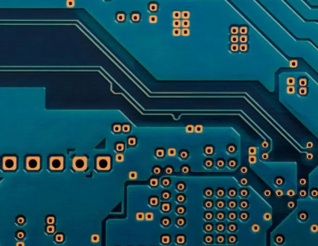
The signal layers contain the copper traces used to route connections between components on the PCB. Most designs will have a minimum of 2 signal layers – one on either side of the board. More complex boards can have 4, 6, or more signal layers stacked up to provide additional routing capability.
The outer layers (Top and Bottom) are often preferred for placing high pin-count components and connectors that need routing to the board’s edge. Inner layers allow traces to pass uninterrupted under components and are ideal for dense routing between chips.
Power and Ground Planes
Power and ground planes provide low-impedance sources of power across the PCB. They act as large areas filled with copper connected to power or ground nets. These planes deliver power more evenly while reducing noise and enhancing signal integrity.
Multiple power planes can be split out to provide different voltages to separate areas of the PCB. For example, a 3.3V power plane may be needed in addition to the main 5V plane for powering logic and analog circuits.
Dielectric Layers
Dielectric layers provide electrical isolation between the conductive copper layers. The dielectric material is typically a resin-reinforced fiberglass such as FR-4. Varying the thickness of the dielectric allows control of the impedance for matched transmission lines.
Other Layer Types
In addition to the core signal, power, and ground layers, PCB stackups include a number of supplemental layers that serve important functions:
Soldermask Layers
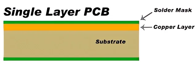
The solder mask (solder resist) is a coat of polymer layer that protects copper traces from oxidation and prevents solder bridges from forming between pads during assembly. Solder mask layers are found on the outer surfaces of the PCB. Openings in the solder mask expose copper pads and traces for soldering.
Silkscreen Layers
Silkscreen layers print text, symbols, and outlines on the PCB for identification. They help identify component footprints, designate pin 1, and provide board info like serial numbers. Silkscreen legend is typically found on the outer surfaces but can also be embedded internally.
Ideal Layer Counts
Determining the right number of layers is an important stackup consideration that balances cost, manufacturability, and electrical performance.
2-Layer Boards
The simplest and most cost-effective PCBs use a 2-layer construction. The top and bottom signal layers suit low complexity designs well. Components can be placed on both sides and vias make vertical connections through the board. Two layers work for many applications but limit routing capacity.
With a top and bottom signal layer plus two internal planes, 4-layer boards offer more flexibility at reasonable cost. The extra routing layers reduce congestion while planes provide solid power distribution. Four layers support more complex layouts.
6+ Layer Boards
High pin-count devices and dense routing often demand PCBs with 6 or more layers. Adding layers provides even greater routing capability and allows more power planes to be dedicated to different voltage levels. While costs increase, the additional layers are warranted for high-speed, high-complexity, or RF designs.
In general, more layers offer better electrical performance but at higher fabrication costs. The layer count should be chosen judiciously based on the design requirements and budget constraints.
Example PCB Stackups
Looking at some common layer stackup configurations helps illustrate how designers choose and sequence layers for different types of boards.
4-Layer Board
A typical 4-layer stackup would be:
Top Signal
Ground Plane
Power Plane
Bottom Signal
This provides a good balance of signal routing on the outer layers along with continuous internal ground and power planes. Two signal layers reduce congestion while the power/ground planes enhance signal integrity.
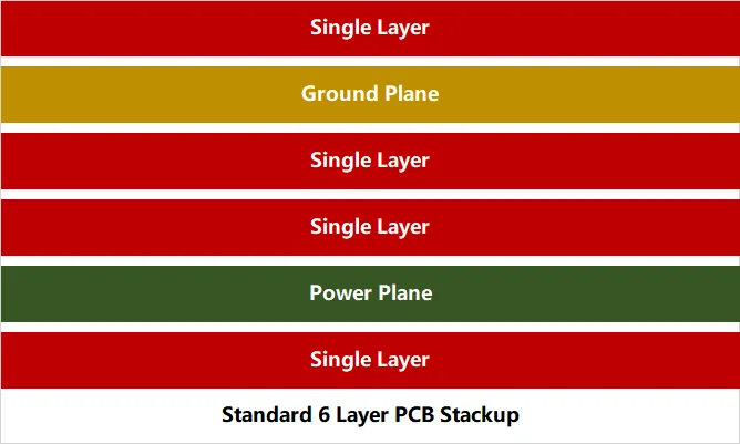
6-Layer Board
A 6-layer stackup allows the addition of a second internal signal layer:
Top Signal
Ground Plane
Signal 2
Power Plane
Signal 3
Bottom Signal
The extra routing layers are useful for high-speed traces or routing dense BGA devices. The sequence keeps reference planes adjacent to each signal layer.
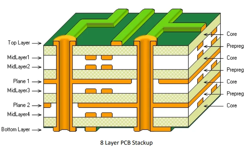
8-Layer Impedance Controlled Board
Where controlled impedances are required, an 8-layer stackup can alternate signal and ground layers:
Top Signal
Ground 1
Signal 2
Ground 2
Signal 3
Ground 3
Signal 4
Bottom Signal
This ensures each signal layer has a reference ground layer above and below with a consistent dielectric thickness. Vias stitch together the ground layers.
FAQs on PCB Layer Stackup
The core layer types are signal layers for routing, power and ground planes for power distribution, and dielectric layers for electrical isolation. Supplementary layers like soldermask and silkscreen add functionality.
Planes provide low-impedance power delivery across the board while also enhancing signal integrity by reducing noise coupling. Planes can be split to isolate different voltage levels.
A typical 4-layer stackup is: Top Signal, Ground Plane, Power Plane, Bottom Signal. This provides two routing layers and continuous power and ground planes.
Designs with high pin count components, dense routing, or high-speed signals benefit from the additional routing layers in a 6-layer board.
Thinner dielectrics allow tighter trace spacing while thicker dielectrics help control impedance over longer traces. Consistent thickness is needed between signal and ground reference layers.
Factors include complexity, routing density, layer type needs, signal integrity, emissions, and fabrication budget. Add layers judiciously based on requirements.
Proper use of ground planes, layer sequencing, and techniques like embedded capacitance can reduce unwanted emissions from the board.
The mechanical layer in a PCB design refers to the physical fiberglass core layers that provide structure and rigidity to the board. Some key points about mechanical layers:
- They are constructed from dielectric materials like FR4, which alternate between the copper layers.
- The thickness and number of mechanical layers impacts the overall thickness and stiffness of the PCB.
- Thicker cores (10+ mils) are used on outer layers for rigidity, while thinner cores (2-6 mils) are common for inner layers.
- Specialized materials like polyimide and metal cores can be used for flexible or rigid-flex PCBs.
- Mechanical drilling is done through the layers to create holes/vias for vertical interconnections.
- The fiber weave and resin percentage impacts mechanical properties like strength and CTE.
- The materials and thickness of the mechanical layers must be compatible with PCB fabrication processes.
- Too few or thin mechanical layers can lead to potential warping or flexing issues.
- Modeling the mechanical structure is important for assessing reliability, thermals, and vibration performance.
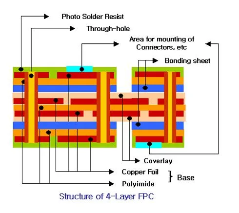
A coverlay is a protective layer that is laminated over the top of flexible PCB circuitry. Some key points about coverlays:
- They provide electrical insulation and protect flexible circuits from environmental damage.
- Coverlays are made from thin, flexible dielectric films like polyimide or polyester.
- Adhesive is used to bond the coverlay securely over the flex circuit traces.
- Openings in the coverlay provide selective access to solder pads and components.
- Coverlays can have single or multiple layers for complex flexible circuits.
- They allow components to be mounted on top of the circuitry underneath.
- Common coverlay thicknesses range from 1-3 mils to maximize flexibility.
- Some coverlay types offer puncture and abrasion resistance for durability.
- Coverlays must withstand flexing stresses as the circuit is bent and shaped.
- They are an essential layer in multilayer flex stackups to isolate circuit layers.
Routing layers refer to the signal layers in a printed circuit board (PCB) stackup that contain the copper traces used to route connections between components. Some key points about routing layers:
- They provide the conductive pathways for signals to travel between pads, pins, and vias on the PCB.
- A PCB will often have multiple routing layers (2, 4, 6+ layers) to provide adequate trace routing capacity.
- Outer routing layers are good for high pin count components and traces that run to board edges.
- Inner routing layers allow traces to pass uninterrupted beneath components and supports high routing density.
- Routing layers follow specific design rules for trace width, spacing, current capacity, and impedance control.
- Critical signals are often routed on inner layers adjacent to a ground plane for shielding.
- Layers are sequenced and stacked to balance routing needs, emissions, signal integrity, etc.
- More routing layers provides increased flexibility and capacity but adds to complexity and cost.
- Advanced HDI PCBs can have 20+ thin routing layers to support high density interconnections.
Related Posts
- Complete Guide for PCB Material
- Types of PCBs: Comprehensive Guide to Printed Circuit Boards
- A Comprehensive Guide to 8 Layer PCB Stackup Design
- PCB Gerber Files – Everything You Need to Know
- Multilayer PCB Design Guide: A Comprehensive Overview
- Rigid Flex PCB Design Guidelines: Key Guidelines to Follow
- High Tg PCB Design Guidelines: Best Practices and Tips for Success
- Design Considerations for Metal Core PCBs: Tips and Tricks for Optimal Performance
- How to Calculate Controlled Impedance for PCB Design?
- What is HDI PCB Stackup – Different Stackups for HDI PCBs
- How to Design a Heavy Copper PCB?