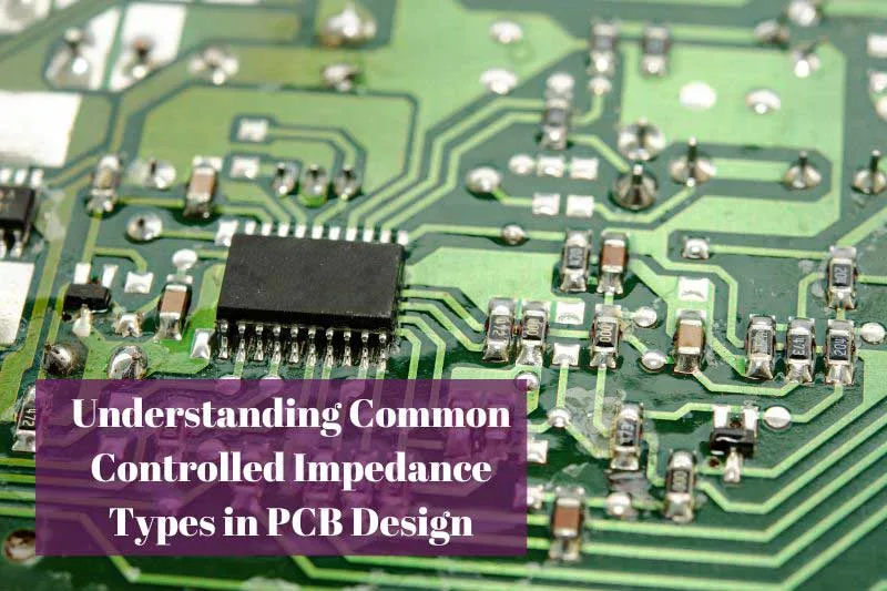
When designing PCBs, one important concept is controlled impedance. This refers to controlling the characteristic impedance of the traces on a PCB to match the impedance requirements of high-speed signals. Proper control of impedance is crucial for signal integrity and to minimize electromagnetic interference (EMI). If the trace impedance is not properly controlled, you can end up with signal reflection, unpredictable current flows, and other issues that impact performance, especially for fast-moving signals.
As a leading PCB manufacturer in China, JHYPCB understands the importance of controlled impedance. In this blog post, we’ll explain the key steps involved in calculating the right trace dimensions to achieve your target controlled impedance in a PCB design. Whether you need 50 ohm, 75 ohm, or other impedance values, we’ll show you how to determine the trace width, height, and other factors. With the right PCB stackup and design, you can maintain impedance across your board for reliable high-speed signals.
What is Impedance and Why is it Important?
Impedance is like the resistance or opposition to the flow of current in a circuit. It is measured in units called ohms. On a PCB, the traces between components act like wires and have a certain impedance.
Controlling the impedance of traces is crucial for several reasons:
- It makes sure the trace impedance matches the impedance of the signals and components it connects. This prevents signal reflection and power loss.
- It helps maintain signal integrity and quality, especially for high-speed signals. Mismatched impedance can distort fast signals.
- It minimizes EMI (electromagnetic interference) that can cause interference between traces.
There are two main types of impedance:
- Differential impedance – This is between two traces with opposite signals, like a differential pair.
- Single-ended impedance – This is the impedance of one trace to the reference ground plane. The most common is 50-ohm or 75-ohm single-ended impedance.
By calculating the right trace width, height, and spacing for your PCB stackup, you can control impedance and match it to your signal requirements. This is key to designing boards with clean, reliable signals.
Factors Affecting Impedance
The impedance of a PCB trace depends on several design elements:
- PCB Stack-up – This refers to the sequence and thickness of the copper, dielectric, and other layers in the board. The stackup affects things like trace height and proximity to the reference plane.
- Trace Width – Wider traces have lower impedance, while thinner traces have higher impedance. So width is used to tune the impedance.
- Trace Spacing – The distance between traces impacts the amount of coupling. Tighter spacing lowers impedance due to capacitive effects.
- Copper Thickness – Thicker copper lowers impedance because of lower resistivity. Trace impedance drops slightly as copper gets thicker.
- Dielectric Constant – Each dielectric material has a constant (Dk) that impacts impedance. The lower the Dk, the higher the impedance. Dk varies with frequency.
By understanding how each of these factors impacts impedance, you can more accurately calculate the trace dimensions needed to achieve your impedance target. The geometry of the trace and the materials around it work together to determine impedance.
How to Calculate Controlled Impedance for PCB?
Step 1: Determine the Required Impedance
The first step in calculating controlled impedance is to determine the required impedance for the trace. The required impedance is usually specified by the system designer or is based on the transmission standard being used. For example, the required impedance for a USB 2.0 trace is 90 Ohms, and for a DDR3 SDRAM interface, it is 50 Ohms.
Step 2: Choose the Trace Geometry and Material
The next step is to choose the trace geometry and material. The geometry includes the width and thickness of the trace, as well as the distance between the trace and the ground plane. The material includes the dielectric constant (Dk) of the PCB substrate. The trace geometry and material affect the controlled impedance of the trace.
Step 3: Calculate the Trace Width
Once the required impedance and trace geometry are determined, the next step is to calculate the trace width. There are several formulas and online calculators that can be used to calculate trace width. The most commonly used formula is the microstrip formula, which is given by:
W = (Zo * t) / (8.85 * Er)^0.5
Where W is the trace width, Zo is the required impedance, t is the thickness of the trace, Er is the dielectric constant of the PCB substrate.
Step 4: Check for Tolerance and Adjustments
After calculating the trace width, it is important to check for tolerance and make adjustments if necessary. The tolerance for controlled impedance is usually specified by the system designer, and it varies depending on the application. If the calculated trace width is outside the tolerance range, adjustments must be made to ensure that the trace impedance is within the required tolerance range.
Step 5: Verify Impedance with Simulation Tools
Finally, it is important to verify the impedance of the trace using simulation tools such as a signal integrity simulator. These simulation tools help to ensure that the calculated impedance is accurate and that the trace will perform as expected.
Conclusion
Controlling impedance is clearly crucial for designing high-speed PCBs that maintain signal integrity. By following the key steps outlined above, you can accurately calculate the trace width, height, and other dimensions needed to achieve your target controlled impedance. Matching the trace impedance to your signals and components prevents reflection, EMI, and other issues.
As you design your stackup, choose your dielectric materials carefully, as the Dk significantly impacts impedance. Wider traces help lower impedance, while closer reference planes raise it. And don’t forget to use an online calculator to verify your impedance calculations.
At JHYPCB, we have extensive experience manufacturing PCBs with controlled impedance for signals up to multi-GHz frequencies. Our engineering team can help you with your impedance design and material selection. We also offer impedance testing services to validate your controlled impedance needs are met.
Contact us today to discuss your next impedance-controlled PCB design and let our expertise in high-speed boards help you succeed. With the right design know-how, you can optimize impedance on your next project.