Your Trusted Prototype PCB Manufacturing And Assembly Partner.
When you partner with us, we do everything to ensure your PCB manufacturing and assembly are completed on time to your specifications with the highest quality.
Leading manufacturer of PCB Fabrication and Assembly in China.
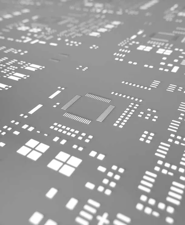
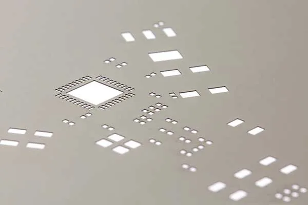
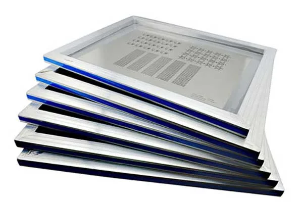
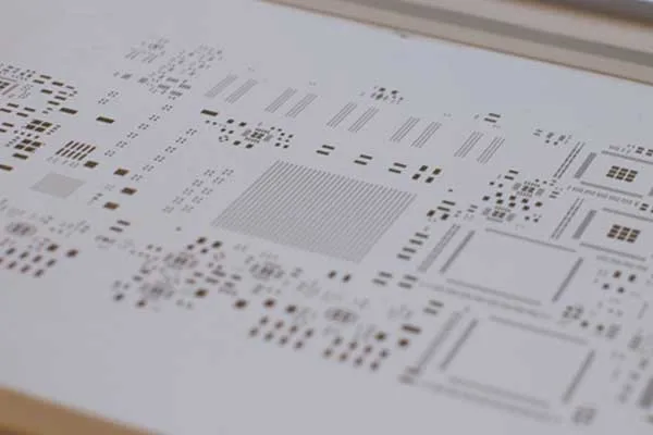
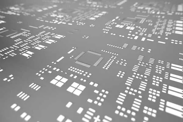
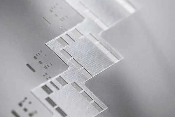
An SMT (Surface Mount Technology) Stencil or PCB Stencil is a thin metal template used to apply solder paste or adhesive onto a printed circuit board during the assembly process. This helps ensure that electronic components are accurately positioned and connected to the PCB. The stencil is placed over the PCB and solder paste is applied through the stencil’s apertures using a squeegee. Once the paste is applied, the stencil is removed and the PCB goes through the reflow oven, where the paste melts and forms a bond between the components and the board.
SMT stencils are typically made of stainless steel or nickel and can be customized according to the specific needs of a project. They come in different types, including frameless stencils, framed stencils, electroformed stencils, prototype stencils and step stencils. The type of stencil used depends on factors such as the size and complexity of the board, the number of components being assembled, and the desired level of accuracy.
SMT stencils play a critical role in the assembly of PCBs by ensuring the precise application of solder paste or adhesive to create strong connections between electronic components and the board.
At JHYPCB, we understand that every PCB assembly project is unique and requires a custom solution. That’s why we offer all types and specifications of SMT stencils for our customers’ specific needs. From laser cut to chemical etched and electroform stencils, our high-quality products ensure precision and accuracy in every project.
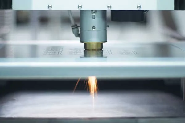
Laser cut SMT stencils use a laser to cut holes into a stainless steel plate in the desired shape. This method is suitable for various volume productions and quick prototyping. The specifications of laser cut SMT stencils are listed below:
| Specification | Description |
|---|---|
| Material | Stainless Steel |
| Thickness | 0.1mm-0.3mm |
| Minimum aperture size | 0.2mm |
| Maximum aperture size | 3mm |
| Circular hole diameter tolerance | ±0.005mm |
| Rectangular hole dimension tolerance | ±0.01mm |
The main features of laser cut SMT stencils include:
Prototype SMT stencils are manufactured by laser cutting and are tailored to your Gerber or CAD files in order to perfectly match your prototype printed circuit board. These solder paste stencils do not have frames and are specifically created for manual printing purposes.
The features of Prototype SMT Stencil are as follows:
Frameless SMT stencils are made from high-quality stainless steel or nickel and have no frame surrounding the stencil. They are designed for use with automatic stencil printers and are ideal for small volume production or prototyping. Their key features include:
| Specification | Frameless SMT Stencils |
|---|---|
| Material | Stainless Steel/Nickel |
| Thickness | 0.08mm to 0.25mm |
| Min. Aperture Size | 0.15mm |
| Max. Board Size | 750 x 600mm |
| Min. Separation Width | 0.1mm |
Framed SMT stencils are made from high-quality stainless steel or nickel and have a frame surrounding the stencil. They provide better stability during printing and are easy to handle, which makes them suitable for medium-to-large volume production. Their key features include:
| Specification | Framed SMT Stencils |
|---|---|
| Material | Stainless Steel/Nickel |
| Frame Size | Various |
| Mesh Count | 80T to 200T |
| Min. Aperture Size | 0.15mm |
| Max. Board Size | 750 x 600mm |
Electroformed SMT stencils are made using an electroforming process and have superior aperture quality compared to framed or frameless stencils. They provide excellent solder paste release, making them ideal for small and fine-pitch components. Their key features include:
| Specification | Electroformed SMT Stencils |
|---|---|
| Material | Nickel |
| Wall Angle | 30 degrees to 45 degrees |
| Opening Size | 0.15mm to 1.5mm |
| Min. Separation Width | 0.1mm |
Chemical etched SMT stencils use a photoresist process and an acid solution to form openings in the desired shape. This method is suitable for various volume productions. The specifications of chemical etched SMT stencils are listed below:
| Specification | Description |
|---|---|
| Material | Stainless Steel |
| Thickness | 0.05mm-0.2mm |
| Minimum aperture size | 0.15mm |
| Maximum aperture size | 3mm |
| Circular hole diameter tolerance | ±0.01mm |
| Rectangular hole dimension tolerance | ±0.02mm |
The main features of chemical etched SMT stencils include:
Step stencils are multi-layered stencils, with each layer having different openings and shapes to apply varying amounts and locations of solder paste at different stages. This stencil design is typically suitable for medium to large volume productions. The specifications of step stencils are listed below:
| Specification | Description |
|---|---|
| Material | Stainless Steel |
| Thickness | 0.05mm-0.2mm |
| Minimum aperture size | 0.15mm |
| Maximum aperture size | 3mm |
| Circular hole diameter tolerance | ±0.01mm |
| Rectangular hole dimension tolerance | ±0.02mm |
The main features of step stencils include:
JHYPCB is a professional PCB manufacturer and assembler with over 12 years of experience in the industry. In addition to their comprehensive PCB manufacturing and assembly services, JHYPCB also offers high-quality SMT stencil production services.
JHYPCB’s SMT stencil production service provides custom-made stencils that are designed to meet the specific needs of their clients. They offer seven different types of SMT stencils, including laser cut, chemical etched, and electroform, etc. Each type has its unique advantages and limitations, allowing clients to choose the most suitable option for their project.
JHYPCB’s SMT stencil production service is an excellent choice for clients who require high-quality stencils for their PCB assembly needs. With our extensive experience in the industry, commitment to quality, and use of state-of-the-art technology, clients can rely on JHYPCB for all their SMT stencil production needs.
| Specifications (width× length, unit: cm) | Effective area (width× length, unit: cm) |
|---|---|
| 37 X 47 | 19 X 29 |
| 30 X 40 | 14 X 24 |
| 42 X 52 | 24 X 34 |
| 45 X 55 | 27 X 37 |
| 58.4 X 58.4 | 38 X 38 |
| 55 X 65 | 34 X 44 |
| 73.6 X 73.6 | 50 X 50 |
| 28 X 38 (without aluminum frame). | 19 X 29 |
| 40 X 60 | 22 X 40 |
| 40 X 80 | 22 X 60 |
| 40 X 100 | 22 X 76 |
| 40 X 120 | 22 X 100 |
| 40 X 140 | 22 X 120 |
| 50 X 70 | 32 X 50 |
| 50 X 80 | 32 X 60 |
| 50 X 120 | 32 X 100 |
| 50 X 140 | 32 X 120 |
| 50 X 150 | 32 X 130 |
| project | Process details |
|---|---|
| Processing technology | Laser cutting |
| Minimal opening | >0.08MM |
| Cutting tolerances | ±0.003MM |
| Steel sheet thickness | NORMAL THICKNESS: 0.1, 0.12, 0.15, 0.18, 0.2MM / SPECIAL THICKNESS: 0.08, 0.06, 0.25, 0.3MM (ADDITIONAL CHARGE) |
| Data format | Gerber、PCB |
| Polishing process | Electrolytic polishing, etching polishing, grinding polishing |
| Steel sheet model | 304HTA |
| Number of machines | 22 laser machines |
| Delivery time setting | 12 hours to 2 days (depending on the order situation) |
JHYPCB’s SMT stencil production service offers the following features:
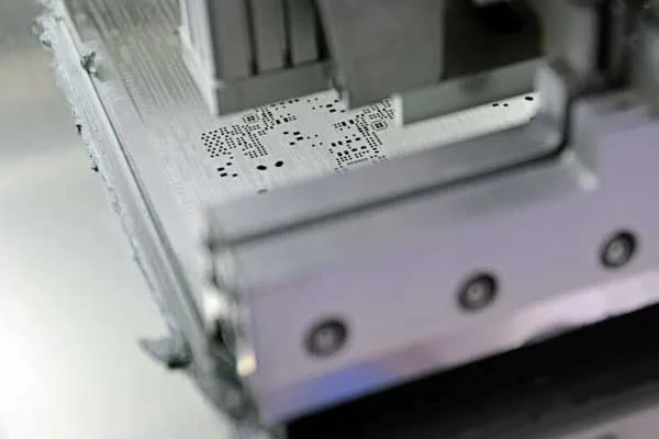
The SMT stencil production process involves several steps that must be followed carefully to ensure high-quality stencils. The following is a detailed description of each step in the process:
The first step in the SMT stencil production process is designing the stencil. This involves creating a CAD (Computer-Aided Design) file that outlines the desired aperture pattern for the stencil. The design should consider the size and shape of the components to be mounted on the PCB, as well as the paste deposit requirements for each component.
Once the stencil design is complete, the next step is selecting the material for the stencil. The most common materials used for SMT stencils are stainless steel and nickel alloy. Stainless steel is more affordable and suitable for most applications, while nickel alloy is more durable and preferred for high-density circuit boards.
The selected material is then cut according to the dimensions specified in the CAD file. There are three different methods of cutting the material, including laser cutting, chemical etching, and electroforming. Each method has its unique advantages and limitations, as described earlier.
After the stencil is cut, it needs to be thoroughly cleaned to remove any debris or residue from the cutting process. This ensures that the stencil remains free of contamination, which can cause defects during the PCB assembly process.
The next step is applying emulsion to the stencil. Emulsion is a photosensitive polymer that is applied to the surface of the stencil. This step is required for chemical etching and electroforming methods only.
Once the emulsion is applied, the stencil is exposed to UV (Ultraviolet) light through a film negative. The areas of the stencil that are not blocked by the emulsion become hardened, while the areas covered by the emulsion remain soft.
After exposure, the stencil is developed by washing it with a solution that dissolves the soft emulsion. This leaves behind an aperture pattern on the stencil that matches the design specified in the CAD file.
The stencil is then thoroughly inspected to ensure that it meets the specifications outlined in the CAD file. Any defects or errors are corrected at this stage to ensure that the stencil is ready for use in PCB assembly.
Once the stencil has been inspected and approved, it is packaged and shipped to the client. The stencil should be handled carefully during shipping to avoid any damage that could affect its performance during PCB assembly.
SMT stencils are essential tools for applying solder paste or adhesive to electronic circuit boards. They offer several benefits over manual application methods, including:
Using an SMT stencil significantly increases the efficiency of the PCB assembly process. By accurately and consistently applying solder paste or adhesive to the board, the stencil helps reduce the time and labor required for hand-soldering each component.
SMT stencils provide better accuracy than manual application methods. The precision of the stencil ensures that the right amount of solder paste or adhesive is applied to each pad, eliminating any potential issues with insufficient or excess material.
Using an SMT stencil also improves the consistency of the PCB assembly process. The stencil ensures that the same amount of solder paste or adhesive is applied to every board, regardless of its size or complexity. This reduces the chances of errors or defects and improves the overall reliability of the final product.
SMT stencils can also help reduce the cost of PCB assembly. By eliminating the need for hand-soldering, the stencil reduces the labor costs associated with assembling each board. Additionally, the consistency and accuracy of the stencil help reduce the amount of wasted materials, further reducing the overall production costs.
SMT stencils can be customized to meet the unique needs of each project. The stencil design can be tailored to accommodate specific components, board sizes, and paste deposit requirements. This ensures that the stencil provides optimal performance for each application.
In conclusion, using an SMT stencil offers numerous benefits over manual application methods, including increased efficiency, better accuracy, improved consistency, reduced cost, and customization. These benefits make the use of SMT stencils essential for any PCB assembly project.
We offer custom SMT stencil production services that are designed to meet the specific needs of each customer. Our extensive experience in the industry and state-of-the-art technology allow us to produce high-quality stencils that meet even the most complex requirements.
Working with us is a straightforward process. Customers can contact us via email, phone, or our online chat service to discuss their specific requirements. Our team will provide expert guidance and advice on the best type of stencil for the application and help create a detailed quote that fits within the customer’s budget.
Once the customer approves the quote, they can upload the necessary files to our secure server. We accept Gerber files, ODB++ files, and other schematic formats. Our team will review the files and provide feedback if any changes need to be made.
After we receive the final file approval, we begin producing the custom SMT stencil according to the specifications provided by the customer. Once the stencil is complete, it is thoroughly inspected to ensure that it meets all the requirements outlined in the customer’s specifications.
To create a custom SMT stencil, we require a CAD file that outlines the desired aperture pattern for the stencil. The most common file formats we accept include:
Our team can provide guidance on which file format is most suitable for the specific project.
In conclusion, our custom SMT stencil production service is designed to provide high-quality stencils that meet the specific needs of each customer. We work closely with customers to ensure that their requirements are met, and accept a wide range of file formats for maximum flexibility. Contact us today to learn more about our custom SMT stencil production services.
JHYPCB offers high-quality SMT assembly services for electronic circuit boards. Our comprehensive services include PCB design, SMT stencil production, component sourcing, and PCB assembly. We use state-of-the-art technology and stringent quality control measures to ensure that our services meet the highest standards of quality and reliability.
We use SMT stencil production as a critical component of our SMT assembly services to ensure that each board is assembled with precision and accuracy. Our custom-made stencils are designed to fit the specific requirements of each project, ensuring optimal performance during the assembly process.
Using SMT stencils helps us achieve high-quality SMT assembly by providing several benefits. First, the stencil ensures that the right amount of solder paste or adhesive is applied to each pad, eliminating any potential issues with insufficient or excess material. Second, the stencil improves the consistency of the assembly process, reducing the chances of errors or defects and improving the overall reliability of the final product.
We use multiple methods for SMT stencil production, including laser cutting, chemical etching, and electroforming. Each method has its unique advantages and limitations, allowing us to choose the most suitable option for each project.
Our SMT assembly services are comprehensive and designed to meet the specific needs of each customer. From PCB design to component sourcing and assembly, we provide end-to-end solutions that ensure optimal results.
Our team of experienced engineers and technicians are dedicated to delivering high-quality services that meet the highest industry standards. We use the latest equipment and technology, rigorous quality control measures, and excellent customer support to ensure that our customers receive the best possible services.
In conclusion, JHYPCB’s SMT assembly services are designed to provide high-quality results that meet the specific requirements of each project. Our use of SMT stencil production is a critical component of our services, ensuring precision, consistency, and reliability during the assembly process. Contact us today to learn more about our SMT assembly services and how we can help with your next project.
A PCB stencil is a tool used in the PCB (Printed Circuit Board) assembly process to apply solder paste or adhesive onto the board's surface for mounting electronic components. The stencil is typically made of stainless steel or nickel alloy and has apertures that are aligned with the pads on the PCB. The apertures ensure that the right amount of solder paste or adhesive is applied to each pad during the assembly process, improving accuracy and consistency. PCB stencils can be custom-made to meet the specific requirements of each project, ensuring optimal performance during the assembly process.
To create a custom SMT stencil, you'll need a CAD file that outlines the desired aperture pattern for the stencil. The file can be in Gerber files, ODB++, or other schematic formats.
Stainless steel and nickel alloy are the most commonly used materials for SMT stencils.
There are three different methods of cutting the material, including laser cutting, chemical etching, and electroforming.
SMT stencils provide precision and accuracy during the assembly process, ensuring that the right amount of solder paste or adhesive is applied to each pad, improving the consistency and reliability of the final product.
JHYPCB offers a comprehensive range of custom SMT stencil production and assembly services, providing state-of-the-art technology and experienced engineers to ensure high-quality results for every project.
The type of SMT stencil required depends on the specific requirements of the project, such as the size and shape of the components to be mounted on the PCB and the paste deposit requirements for each component. Our team can provide expert guidance and advice on the best type of stencil for your application.
The lead time for custom SMT stencil production can vary depending on the complexity of the project and the chosen production method. Typically, it takes anywhere from 24 hours-2 working days to produce a custom SMT stencil.
Yes, SMT stencils can be reused multiple times but require proper maintenance and cleaning after each use to ensure optimal performance.
The cost for custom SMT stencil production varies depending on the stencil's size, complexity, and required material. Contact us today for a customized quote that fits within your budget.
Yes, we offer expedited services for urgent projects. Please contact us with your specific requirements, and our team will work with you to provide the fastest possible turnaround time.
When you partner with us, we do everything to ensure your PCB manufacturing and assembly are completed on time to your specifications with the highest quality.
Fill out the form below, and we will get back to you within the next 24
hours to complete the order, and then you’re all set to get started!
Prefer to email? Feel free to contact us directly at sales@pcbjhy.com.