


Your Trusted Prototype PCB Manufacturing And Assembly Partner.
When you partner with us, we do everything to ensure your PCB manufacturing and assembly are completed on time to your specifications with the highest quality.
Leading manufacturer of PCB Fabrication and Assembly in China.
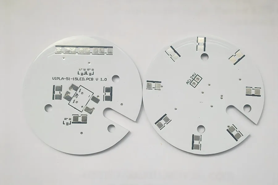
Flexible aluminum PCBs feature an aluminum core layered with dielectric and conductive layers that allow the board to flex and bend. The aluminum, typically an alloy like 5052 or 6061, provides thermal conductivity while maintaining mechanical strength and durability. The dielectric is polyimide, which withstands bending and flexing motion.
Key Characteristics

A Flexible Aluminum PCB’s stack up or structure can vary depending on the specific design requirements and application needs. However, in general, a flexible aluminum PCB typically consists of the following layers:
Base Material: The base material of the flexible aluminum PCB is usually made of polyimide, a high-temperature resistant and flexible polymer material.
Conductive Layers: The conductive layers are made of thin sheets of aluminum, which provide high thermal conductivity and excellent electrical performance.
Solder Mask Layer: The solder mask layer is a protective layer that covers the conductive traces and pads on the PCB, preventing oxidation and corrosion of the metal surfaces.
Coverlay Layer: The coverlay layer is a flexible polymer material that provides a protective coating over the top of the PCB, protecting it from damage during handling and use.
Typical flex aluminum PCB construction:
The fabricated boards can flex up to a minimum bend radius of 10 times the total board thickness. The flexing improves reliability by absorbing stresses.
In some cases, additional layers may be added to the stack up of a flexible aluminum PCB, such as adhesives, insulating layers, or additional conductive layers for multi-layer designs.
It’s important to note that a flexible aluminum PCB’s stack up or structure is critical to its performance and reliability and must be carefully designed and manufactured to meet the application’s specific requirements.
Flexible Aluminum PCB has several unique characteristics and advantages compared to traditional rigid PCBs. Some of the key characteristics and advantages of Flexible Aluminum PCBs are:
Flexibility: Flexible Aluminum PCBs can be bent, twisted, and folded without damaging the circuitry or the board itself. This flexibility allows for the creation of unique shapes and sizes, making it ideal for applications where space is limited.
High Thermal Conductivity: The aluminum substrate used in Flexible Aluminum PCBs has excellent thermal conductivity, allowing for efficient dissipation of heat generated by high-power components. This feature is especially important in applications such as LED lighting, automotive electronics, and power electronics.
Light Weight: Flexible Aluminum PCBs are lightweight, which makes them an ideal choice for products that require a high degree of portability, such as wearable devices or portable medical equipment.
High Durability: The use of high-quality materials and manufacturing processes in Flexible Aluminum PCBs ensures high durability, which makes them less prone to damage from vibration, shock, or impact.
Cost-Effective: Despite their unique characteristics and advantages, Flexible Aluminum PCBs can be cost-effective due to their ability to reduce material usage and increase manufacturing efficiency.
Increased Design Flexibility: Flexible Aluminum PCBs provide greater design flexibility compared to traditional rigid PCBs, allowing designers to create more complex and unique designs that would otherwise be impossible to achieve.
Reduced Assembly Time: Flexible Aluminum PCBs can be assembled quickly and efficiently, reducing assembly time and making them ideal for high-volume production.
Flexible Aluminum PCB has numerous applications due to its unique characteristics and advantages. Some of the common applications of Flexible Aluminum PCBs include:
LED Lighting: Flexible Aluminum PCBs are used extensively in LED lighting applications due to their high thermal conductivity, which allows for efficient dissipation of heat generated by high-power LED components.
Automotive Electronics: Flexible Aluminum PCBs are used in automotive electronics for their high durability and ability to withstand vibration, shock, and extreme temperatures.
Wearable Devices: Flexible Aluminum PCBs are an ideal choice for wearable devices due to their flexibility, lightweight, and compact size.
Medical Devices: Flexible Aluminum PCBs are used in medical devices for their high durability, reliability, and resistance to harsh chemicals and sterilization processes.
Consumer Electronics: Flexible Aluminum PCBs are used in a wide range of consumer electronics, including smartphones, tablets, and laptops, for their ability to reduce space requirements and improve performance.
Aerospace and Defense: Flexible Aluminum PCBs are used in aerospace and defense applications due to their high reliability, resistance to harsh environments, and ability to reduce weight and size requirements.
Power Electronics: Flexible Aluminum PCBs are used in power electronics for their high thermal conductivity, which allows for efficient dissipation of heat generated by high-power components.
Overall, the unique characteristics and advantages of Flexible Aluminum PCBs make them an excellent choice for a wide range of applications in various industries.
The manufacturing process of Flexible Aluminum PCB involves several steps, including:
Designing: The first step in the manufacturing process of Flexible Aluminum PCBs is designing the PCB layout using computer-aided design (CAD) software. The layout specifies the location of components, traces, and other features on the PCB.
Material Selection: The next step is selecting the appropriate materials for the PCB, including the base material, conductive layers, solder mask, and coverlay. The materials used depend on the specific requirements of the application.
Drilling: The PCB layout is transferred to a copper-clad aluminum sheet, and holes are drilled in the sheet at locations specified in the design. These holes are used for component placement and electrical connections.
Etching: After drilling, the copper layers are etched to remove the unwanted portions, leaving only the conductive traces and pads.
Lamination: The base material, conductive layers, and coverlay are laminated together using heat and pressure, forming a multilayered PCB.
Solder Mask Application: A solder mask is applied to the surface of the PCB, covering the exposed copper traces and pads to prevent oxidation and corrosion.
Surface Finishing: The surface of the PCB is finished with a protective coating, such as gold, silver, or nickel, to enhance its durability and prevent oxidation.
Testing and Inspection: The finished Flexible Aluminum PCB is tested and inspected to ensure its electrical and mechanical performance meets the design specifications.
Flexible Aluminum PCB has specific technical parameters and requirements that need to be considered during the design and manufacturing process. Some of the key technical parameters and requirements of Flexible Aluminum PCBs are:
Thickness: The thickness of the Flexible Aluminum PCB should be specified based on the application requirements. Generally, the thickness of the base material ranges from 0.1mm to 3mm, and the overall thickness of the PCB can range from 0.2mm to 3mm.
Copper Thickness: The thickness of the copper layer on the Flexible Aluminum PCB should be specified based on the current-carrying capacity and the application requirements. Generally, the copper thickness can range from 0.5oz to 10oz.
Minimum Trace Width/Spacing: The minimum trace width and spacing on the Flexible Aluminum PCB should be specified based on the application requirements and the manufacturing process. The minimum trace width and spacing can range from 0.1mm to 0.3mm.
Surface Finish: The surface finish on the Flexible Aluminum PCB should be specified based on the application requirements and the manufacturing process. Common surface finishes include HASL, ENIG, OSP, and immersion tin.
Thermal Conductivity: The thermal conductivity of the aluminum substrate used in Flexible Aluminum PCBs is an important parameter that needs to be considered for applications that generate a significant amount of heat.
Peel Strength: The peel strength of the coverlay used in Flexible Aluminum PCBs should be specified based on the application requirements. The peel strength should be high enough to prevent delamination during use.
Bend Radius: The bend radius of the Flexible Aluminum PCB should be specified based on the application requirements. The minimum bend radius should be specified to prevent damage to the circuitry during bending or flexing.
Tensile Strength: The tensile strength of the coverlay and the adhesive used in Flexible Aluminum PCBs should be specified based on the application requirements. The tensile strength should be high enough to prevent tearing or damage during use.
Overall, the technical parameters and requirements of Flexible Aluminum PCBs are critical to ensuring that the PCB meets the specific requirements of the application and performs reliably over its expected lifespan.
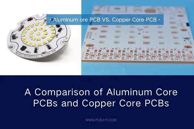
| – | Flexible PCB | Flexible Aluminum PCB |
|---|---|---|
| Material | Typically made of polyimide or polyester film with copper conductors | Made of aluminum substrate with copper conductors |
| Thickness | Generally thinner and more lightweight | Thicker and heavier |
| Thermal Conductivity | Poor thermal conductivity | High thermal conductivity |
| Mechanical Strength | Less rigid and more flexible, making them suitable for curved or irregularly shaped devices | More rigid and less flexible, making them more suitable for flat or straight devices |
| Cost | Generally less expensive than flexible aluminum PCBs | More expensive than flexible PCBs |
| Applications | Commonly used in consumer electronics, medical devices, and aerospace industries | Typically used in automotive, industrial, and military applications that require high thermal conductivity and mechanical strength |
Overall, flexible PCBs and flexible aluminum PCBs have different characteristics and are suitable for different applications. Flexible PCBs are more lightweight, flexible, and less expensive, making them a good choice for consumer electronics and medical devices. On the other hand, flexible aluminum PCBs are more expensive but offer high thermal conductivity and mechanical strength, making them more suitable for automotive, industrial, and military applications.
Our company provides comprehensive manufacturing services for Flexible Aluminum PCBs for various applications. Our manufacturing services include:
Design Support: We provide design support services to our customers to ensure that the PCB layout and design meet the specific requirements of their application. Our experienced engineers can work closely with customers to optimize the PCB layout and design for optimal performance and reliability.
Material Selection: We work with our customers to select the appropriate materials for their PCB based on their specific requirements. Our materials include high-quality base materials, conductive layers, solder masks, and coverlay.
Manufacturing Capabilities: Our state-of-the-art manufacturing facility has advanced manufacturing capabilities that enable us to produce high-quality Flexible Aluminum PCBs with fast turnaround times. Our capabilities include drilling, etching, lamination, surface finishing, and testing.
Quality Control: We have a strict quality control process in place to ensure that our Flexible Aluminum PCBs meet the highest standards of quality and reliability. Our quality control process includes visual inspection, electrical testing, and mechanical testing.
Customization: We offer customization services to our customers to meet their unique requirements. Our customization services include specific PCB thickness, copper thickness, surface finish, and other technical parameters.
Competitive Pricing: We offer competitive pricing for our Flexible Aluminum PCB manufacturing services without compromising on quality. Our pricing is based on the customer’s specific requirements, and we offer flexible pricing options to accommodate different budget requirements.
As a professional PCB manufacturer, JHYPCB provides innovative PCB solutions, including single-sided, double-sided, and multilayer aluminum PCBs, flexible aluminum PCBs, and flexible PCBs with up to 12 layers. We meet the needs of complex applications. Leveraging decades of PCB technical expertise, we are committed to delivering high-quality PCB products and one-stop services. If you have any PCB requirements, please contact our sales team immediately at sales@pcbjhy.com to discuss custom solutions. We can fulfill PCB orders from prototyping to high-volume production, supporting your project’s success. Contact JHYPCB today to experience the professional service of a premium PCB manufacturer!


When you partner with us, we do everything to ensure your PCB manufacturing and assembly are completed on time to your specifications with the highest quality.
Fill out the form below, and we will get back to you within the next 24
hours to complete the order, and then you’re all set to get started!
Prefer to email? Feel free to contact us directly at sales@pcbjhy.com.