


Your Trusted Prototype PCB Manufacturing And Assembly Partner.
When you partner with us, we do everything to ensure your PCB manufacturing and assembly are completed on time to your specifications with the highest quality.
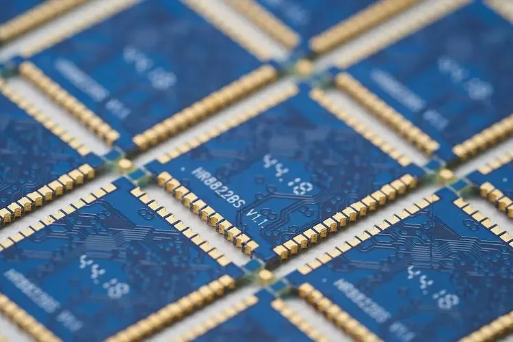
Leading manufacturer of PCB Fabrication and Assembly in China.
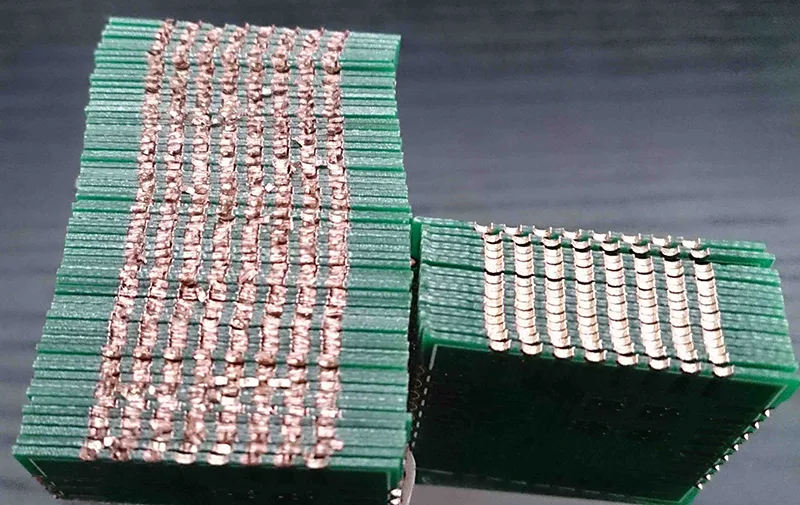
Plated half-holes, also called castellated holes, are a kind of drilled hole that runs along the edges of a rigid PCB board that goes through plating, and then it is milled halfway. These small cutouts or notches are plated with barrel walls, allowing electrical connections between different layers of the PCB. Plated half-holes are commonly found on WiFi modules that are soldered onto larger PCBs, similar to ICs. They are typically used in board-to-board connections, especially when joining two PCBs that use different technologies. Plated half-holes offer a variety of benefits for electronic applications. For example, they can be helpful when utilizing surface-mount components that need to be soldered onto the edge of the board, or for creating semi-permanent mechanical connections between two boards. Engineers can also take advantage of plated half-holes when dealing with constrained space or other design limitations.
In the past, if one needed to connect a daughter board to a mother board, a board-to-board connector was required. However, this added bulk and increased the project cost. Now, with the plated half-holes technique, one can remove the connector, making PCB assembly much easier and more economical.
Plated half-holes, located on the boundaries of a PCB, act as solder mounting device (SMD) terminal pads. Direct soldering and connection to the mother PCB make the entire system considerably thinner than a comparable connection with multi-pin connectors. Not only is this an economical connection technique, but it also allows the circuit board to be converted into a surface-mounted assembly.
Furthermore, plated half-holes provide a better landing for soldering as they are concave and plated. Overall, the use of plated half-holes as a board-to-board connection technique offers numerous benefits for PCB assembly and design.
Half-holes are designed differently in various CAD software, but the desired result in Gerber files should follow these guidelines. Plated-thru holes (vias) should be added in rows on the board boundaries where half vias are required. A 1/2 circle of plated holes should be present on the board body, while another 1/2 circuit should be present on the outside of the outline.
In addition, the following elements should be included in your Gerber files zip folder:
Here are some guidelines to follow when designing plated half-holes:
Ensure that the center point of each plated half-hole is precisely placed on the edge or outline of the PCB. For oval-shaped holes, pay attention to the start and end points.
It is crucial to define these holes as plated through-holes in your EDA application.
If you are uploading Gerber files, make sure to include the holes/slots in the drill file, such as *.drills_pth.xln file, *pth.drl file.
Each plated half-hole must be within a pad on each copper layer (including inner layers for a 4-layer board) to ensure proper stability of the copper sleeve.
Make sure the pad fully surrounds the hole. The requirements for pads and annular rings are the same as for regular through-holes.
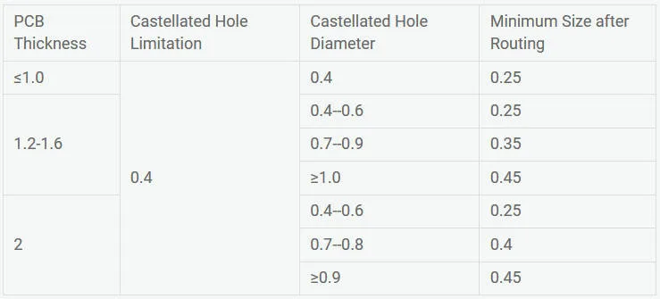
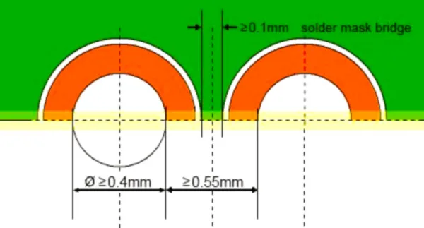
The minimum half-hole diameter is typically 0.6mm, but JHYPCB accepts a minimum half-hole diameter of 0.4mm.
The minimum edge-to-edge spacing between holes should be 0.55mm. If it is between 0.47mm and 0.55mm, there will be an increase in the price and lead time.
Lastly, ensure that the minimum solder mask bridge size is 0.1mm.
Please consult the provided form for specific details, with all measurements in millimeters.
Plated half-holes can be manufactured for both prototype and high-volume PCBs at JHYPCB, without compromising quality and increased PCB design flexibility. Our advanced manufacturing process ensures a guaranteed yield, except for general rules that apply to all PCB designs such as restrictions on shape and panel layout.
To create plated half-holes, the standard whole vias are made at the edge of the boards, then cutting the holes in half using a milling tool. It’s important to use heavy-duty milling bits that can handle the hardness of the copper wall to prevent breakage at high speeds and ensure a smoother finish. After milling, all half-holes undergo inspection and deburring according to our quality control standards.
To connect the castellated PCB to other modules through board-to-board soldering, it is necessary to have plated half-holes. The holes are positioned at the edge of the module and are half in size, making it easy to access and solder them. Having SMD pads beneath a module creates an obstacle during component placement, whereas holes on the side of the PCB reduce alignment errors. Plated half-holes simplify measurement of distances between the holes and solder, allowing for easier measurements even after module placement. Additionally, since the PCB modules with castellated holes are surface-mount sub-assemblies, they can fit directly onto another circuit board, resulting in a cleaner surface without any dust or dirt accumulation in between.
Plated half-holes offer several advantages. Firstly, they are easily accessible and simple to solder since they are located on the side of the module. This is in contrast to having SMD pads on the bottom of the module, which can make component installation difficult. Additionally, measuring the distance between the hole and the solder becomes much easier when using plated half-holes, and even after the module is placed calipers can be used for this purpose. If the pads were located beneath the module, such measurements would be impossible. Furthermore, the chances of misalignment are reduced when using plated half-holes on the side of the PCB, as compared to having pads on the bottom of the module. Finally, PCB modules with plated half-holes are surface-mountable components which can be mounted on another circuit board, similar to SMD components. This tight connection helps to prevent the accumulation of dust and debris between the boards.
Plated half-holes are a type of circuit board hole that is drilled halfway through the board's thickness and then plated with copper to create a conductive connection.
PCBs that have high-density designs, multi-layered boards, embedded components, and boards that require high strength and reliability are some examples of PCBs that can benefit from using plated half-holes.
The recommended diameter of plated half-holes is 0.25-0.5mm, and the recommended depth is 0.3-0.35mm.
The steps involved in manufacturing plated half-holes include drilling the hole, creating a copper barrel, cleaning the hole, and plating the hole.
The quality of plated half-holes can be ensured by implementing proper design rules, manufacturing processes, and quality control measures such as inspection and testing.
Yes, plated half-holes can be used for high-speed signal transmission if the design and manufacturing processes are done properly.
Yes, plated half-holes can be used for thermal vias, and they provide better thermal dissipation compared to standard vias.
Plated half-holes are tested during inspection using electrical testing methods, such as continuity and isolation testing, to ensure that the connections are properly made and there are no shorts or open circuits.
Do you still require assistance? Please reach out to us at sales@pcbjhy.com if you have any further questions or inquiries. Are you in need of a quote for a PCB or PCBA? Request a quote now.
When you partner with us, we do everything to ensure your PCB manufacturing and assembly are completed on time to your specifications with the highest quality.
Fill out the form below, and we will get back to you within the next 24
hours to complete the order, and then you’re all set to get started!
Prefer to email? Feel free to contact us directly at sales@pcbjhy.com.