


Your Trusted Prototype PCB Manufacturing And Assembly Partner.
When you partner with us, we do everything to ensure your PCB manufacturing and assembly are completed on time to your specifications with the highest quality.
Leading manufacturer of PCB Fabrication and Assembly in China.
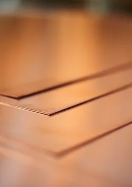
PCB copper foil is a special material used for PCB manufacturing. PCB copper foil is a thin layer of copper laminated onto a substrate material to create conductive traces or pads on a PCB. The copper foil is etched away in certain areas to form the desired circuit pattern. The thickness, width, and quality of the copper foil are important factors that affect the electrical performance and reliability of the PCB.

It is important to select the appropriate type of PCB copper foil depending on the specific application requirements of the PCB being manufactured. Factors to consider include the operating frequency of the circuit, the thermal requirements of the application, and the flexibility requirements of the PCB.
According to different classification methods, PCB copper foil also has the following types:
PCB copper foil thickness refers to the thickness of the layer of copper that is applied to the substrate material of a printed circuit board. This thickness can vary depending on the requirements of the particular PCB design, and it is an important factor to consider when designing a PCB, as it can affect the electrical performance, signal integrity, and cross-talk of the board.
The copper foil thickness is typically measured in ounces (oz). One ounce refers to the thickness of copper that evenly covers an area of one square foot, which is approximately 1.4 mils, expressed in weight per unit area. The formula for this is 1oz=28.35g/FT2, where FT2 represents square feet and one square foot equals 0.09290304 square meters. Additionally, there are other common measurement units for copper foil thickness, such as microns and millimeters. These different units can be converted between each other using conversion formulas.
There are several standard copper thickness options that are commonly used in PCB manufacturing. These include:
The thickness of the copper layer selected for a particular PCB should take into account the amount of current the board needs to carry, the distance between traces, and the amount of heat the board is expected to generate, among other factors.
If the copper thickness selected is too thin, there may be issues with impedance and voltage drop, which can negatively impact the performance of the PCB. On the other hand, if the copper thickness selected is too thick, it can be more difficult to etch the traces and vias, which can increase the cost of manufacturing.
PCB designers need to carefully evaluate the requirements of their particular design to determine the appropriate copper thickness for their board, taking into account factors such as the size and complexity of the board, the expected electrical loads, and the manufacturing process used.
If not stated differently in the procurement documentation, the minimum total thickness of copper conductors (including copper foil and copper plating) after processing must comply with Table 3-1 in IPC-A-600G.
Table 3-1 External Conductor Thickness after Plating
| Weight | Absolute Cu Min. (IPC-4562 less 10% reduction) (μm) [μin] | Plus Min. Plating for Class 1 & 2 (20μm) [787μin] | Plus Min. Plating for Class 3 (25μm) [984μin] | Max. Variable Processing Allowance Reduction* (μm) [μin] | Min. Surface Conductor Thickness after Processing (μm)[μin] | |
| Class 1 & 2 | Class 3 | |||||
| 1/8oz | 4.60 [181] | 24.60 [967] | 29.6 [1,165] | 1.50 [59] | 23.1 [909] | 28.1 [1,106] |
| 1/4oz | 7.70 [303] | 27.70 [1,097] | 32.70 [1,287] | 1.50 [59] | 26.2 [1,031] | 31.2 [1,228] |
| 3/8oz | 10.80 [425] | 30.80 [1,213] | 35.80 [1,409] | 1.50 [59] | 29.3 [1,154] | 34.3 [1,350] |
| 1/2oz | 15.40 [606] | 35.40 [1,394] | 40.40 [1,591] | 2.00 [79] | 33.4 [1,315] | 38.4 [1,512] |
| 1oz | 30.90 [1,217] | 50.90 [2,004] | 55.90 [2,201] | 3.00 [118] | 47.9 [1,886] | 52.9 [2,083] |
| 2oz | 61.70 [2,429] | 81.70 [3,217] | 86.70 [3,413] | 3.00 [118] | 78.7 [3,098] | 83.7 [3,295] |
| 3oz | 92.60 [3,646] | 112.60 [4,433] | 117.60 [4,630] | 4.00 [157] | 108.6 [4,276] | 113.6 [4,472] |
| 4oz | 123.50 [4,862] | 143.50 [5,650] | 148.50 [5,846] | 4.00 [157] | 139.5 [5,492] | 144.5 [5,689] |
Reference:
The minimum copper foil thickness (or conductor thickness) represents the highest coplanar thickness that can conduct electric current. Such thickness includes individual scratches, but excludes the saw-toothed dendritic surface that promotes adhesion of the metal-clad surface.
For the minimum internal layer copper foil thickness after processing, Table 3-2 in IPC-A-600G must be followed.
Table 3-2 Internal Layer Foil Thickness after Processing
| Weight (oz) [μm] | Absolute Cu Min. (IPC-4562 less 10% reduction) (μm) [μin] | Max. Variable Processing Allowance Reduction* (μm) [μin] | Min. Final Finish after Processing (μm)[μin] |
| 1/8 [5.10] | 4.60 [181] | 1.50 [59] | 3.1 [122] |
| 1/4 [8.50] | 7.70 [303] | 1.50 [59] | 6.2 [244] |
| 3/8 [12.00] | 10.80 [425] | 1.50 [59] | 9.3 [366] |
| 1/2 [17.10] | 15.40 [606] | 4.00 [157] | 11.4 [449] |
| 1 [34.30] | 30.90 [1.217] | 6.00 [236] | 24.9 [980] |
| 2 [68.60] | 61.70 [2,429] | 6.00 [236] | 55.7 [2,193] |
| 3 [102.9] | 92.60 [3,646] | 6.00 [236] | 86.6 [3,409] |
| 4 [137.20] | 123.50 [4,862] | 6.00 [236] | 117.5 [4,626] |
| Above 4 [137.20] | – | 6.00 [236] | 6μm [236μin] below minimum thickness of calculated 10% reduction of foil thickness in IPC-4562 |
Notes:
At JHYPCB, we take pride in providing a wide range of copper weights to meet your requirements for copper thickness, particularly for thick copper PCBs. We offer a variety of options, including 12μm (1/3oz), 18μm (1/2oz, or H oz), 35μm (1oz), 70μm (2oz), 105μm (3oz) and 210μm (4oz), enabling you to select the perfect match for your application.
Our selection of copper weights allows us to provide flexible and reliable solutions to meet your needs. Whether you require a thin copper layer, a high-density interconnect PCB with thicker copper weights or a board with varying copper thickness, JHYPCB has the expertise and capabilities to deliver quality products that meet your specific requirements.
PCB Copper foil is widely used in various fields such as electronics, power transmission and communication systems due to its unique combination of chemical, physical, and electrical properties. Its high conductivity, resistance to corrosion, smoothness, and ease of adhesion to substrates make it an ideal choice for electronic applications. Additionally, its malleability, flexibility, and high melting point enable it to be easily manipulated and formed to fit specific design requirements. PCB Copper foil’s low resistance, high thermal conductivity, low dielectric constant, and low dielectric loss also make it ideal for electrical applications.
Chemical Characteristics:
Physical Characteristics:
Electrical Characteristics:
PCB copper foil used in the industry is more complex than one would imagine. Copper is an excellent conductor and thermal conductor, making it an ideal material for most PCB conductors. Copper foils also have many other characteristics, which are important for engineers to understand.
There are generally two types of copper foil used in the PCB industry: rolled annealed copper (RA) and electrolytic deposition (ED) copper foil. The manufacturing process of RA copper foil starts from pure copper stock, and the thickness is reduced by continuous rolling until it reaches the desired thickness. The ED copper foil is made by electroplating copper onto a rotating titanium drum, and the thickness of the foil depends on the speed of the drum rotation. After manufacturing, both RA and ED copper foils require multiple processing steps.
Copper foil has various processing methods, including passivation treatment that aims to prevent oxidation before use. Other methods aim to enhance the chemical adhesion of copper foil to certain resin systems, such as PPE and PTFE. Different resin systems react differently to each processing method due to their distinct bonding characteristics. Some processing/resin combinations are better than others and achieve good adhesion. Some processing methods can ensure appropriate adhesion at high temperatures, and others can ensure reliable adhesion surfaces for long-term high-temperature applications.
For rigid PCB applications, ED copper foil is most commonly used, but RA copper foil is also used. Generally, RA copper foil is more expensive than ED copper foil unless certain features of RA copper foil have a greater advantage for the application. RA copper foil has a very smooth surface, which is conducive to low insertion loss, making it suitable for high-frequency and high-speed digital applications. RA copper foil has a unique manufacturing process, resulting in in-plane crystal structure, which is advantageous for applications that require circuit bending. However, the downside of RA copper foil is related to this crystal structure, that is, etching of small circuit features, which can be overcome to some extent by using specific etching for RA copper foil.
ED copper foil is widely used in the PCB industry. There are different types of ED copper foil, which are categorized according to their surface roughness and/or processing methods. IPC classifies ED copper foil into different categories based on their roughness, including LP (low profile), VLP (very low profile), and HVLP (extremely low profile).
PCB Copper Foil has a wide range of applications in the PCB manufacturing industry, including:
In summary, PCB Copper Foil plays an essential role in the PCB manufacturing industry, providing high conductivity, signal transmission, and system performance for various PCB applications.
A. Considerations for selecting PCB copper foil:
B. Performance indicators of PCB copper foil:
Recommendations for selecting PCB copper foil:
PCB Copper Foil is a thin layer of copper that is used to create electrical conductive pathways on the surface of circuit boards. Its main characteristics include exceptional electrical conductivity, thermal conductivity, and corrosion resistance.
There are different types of Copper Foil available for PCB designs, including rolled annealed (RA) Copper Foil, electrodeposited (ED) Copper Foil, and treated ED Copper Foils.
When working with Copper Foil during the PCB manufacturing process, special precautions such as proper handling, storage, and protection against oxidation may be necessary to ensure the quality and integrity of the material.
Both RA (Rolled Annealed) copper and ED (Electro-Deposited) copper are commonly used for flex PCB substrates.
RA copper is a type of copper foil that is annealed, meaning it undergoes heat treatment to improve its flexibility and ductility. RA copper is suitable for flex PCB substrates because it is more malleable and can better conform to the flexible substrate material.
ED copper, on the other hand, is deposited onto a surface using an electrochemical process. It is a very pure copper with a very smooth surface finish, which can result in better circuit accuracy, but it is typically stiffer and less ductile than RA copper.
In general, RA copper is a popular choice for flex PCB applications due to its increased flexibility and conformity to the substrate.
"PCB copper foil current carrying capacity" refers to the maximum amount of electrical current that a copper foil on a printed circuit board (PCB) can handle without any damage or loss of performance. The current carrying capacity of a PCB copper foil depends on various factors such as its thickness, width, and ambient temperature. It is an important design consideration because using a copper foil with a lower current carrying capacity than what is necessary can result in heat generation, voltage drops, and other issues.
The relationship between PCB copper foil thickness, line width, and current is complex, but it can be summarized as follows:
The thicker the copper foil, the more current it can carry without overheating and melting. This is because the thickness of the copper foil affects its resistance, and thicker foils have lower resistance.
The width of the copper trace also affects its ability to carry current. Wider traces have lower resistance and can therefore carry more current without overheating. However, wider traces also take up more space on the board, which can be a limiting factor in some applications.
Current carrying capacity is also affected by factors such as the ambient temperature and the amount of heat sinking provided by the board and its components. In high current applications, it is important to choose copper foil thickness and trace width that will allow the current to flow without causing overheating or other problems.
In general, designers should select PCB copper foil thickness and trace width based on the expected current load and the space available on the board. They should also consider factors such as thermal management and the overall requirements of their application.
When you partner with us, we do everything to ensure your PCB manufacturing and assembly are completed on time to your specifications with the highest quality.
Fill out the form below, and we will get back to you within the next 24
hours to complete the order, and then you’re all set to get started!
Prefer to email? Feel free to contact us directly at sales@pcbjhy.com.