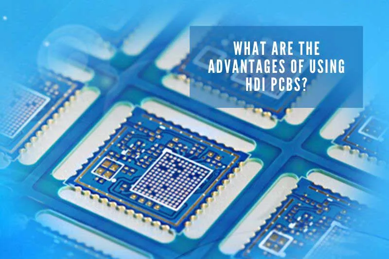
HDI PCBs are all the rage today for packing more components and functionality into increasingly smaller electronic devices. HDI PCBs achieve this incredible miniaturization by utilizing thinner dielectrics, finer lines and spaces, smaller vias, and higher wiring density.
But hidden beneath every compact HDI PCB lies its secret weapon – the layer stackup. This refers to the sequence of dielectric, conductive, and resistive layers laminated together into a PCB substrate.
The layer stackup profoundly affects HDI PCB performance. A good stackup allows traces to route cleanly without interference while a bad stackup leads to signal loss and crosstalk. That’s why optimizing the layer stackup configuration is critical when designing HDI PCBs.
In this article, we will demystify HDI PCB layer stackups by exploring popular configurations like 4-layer, 6-layer, and complex multilayer stackups. We’ll also discuss key stackup design considerations like signal integrity, EMI control, and heat dissipation.
By learning what goes into designing different HDI PCB stackups and why they matter, you’ll be better equipped to architect the optimal stackup for your next HDI PCB project, no matter how demanding the application!
Basic HDI Stackups
Let’s first look at a couple straightforward HDI PCB stackup configurations that provide a foundation for many designs:
- 4-Layer HDI Stackup
The 4-layer stackup is the simplest option for an HDI PCB. It consists of the outer top and bottom signal layers, with a power plane and ground plane in the inner layers 2 and 3.
The power and ground planes provide shielding and impedance control for traces on the signal layers. Four layers give decent routing flexibility while keeping stackup thinness optimal for HDI capability.
- 6-Layer HDI Stackup
This adds two more signal layers to the 4-layer stackup. The additional layers allow the routing more traces, especially for designs with high I/O counts. The sequence is generally top and bottom signal layers, power and ground planes, and signal layers in the core.
The 6-layer HDI stackup improves signal isolation by embedding traces between power and ground. This helps minimize crosstalk and EMI. The disadvantage is slightly increased thickness and cost over 4 layers.
These basic HDI stackups offer a practical balance of layer count, electrical performance and cost. They serve as good starting points for many common applications.
Complex HDI PCB Stackups
For advanced HDI PCB applications like servers, network switches, and aerospace avionics, more complex stack-ups are often required:
- 8+ Layer Stackups
Mission-critical systems may utilize HDI stackups with 8, 12, or even 16+ layers. This enables extensive routing capacity with strict segregation across layer boundaries. Separate layers can isolate critical control signals, high-speed data lanes, and RF circuits. - Hybrid Multilayer Stackups
Hybrid designs combine conventional through-hole technology on outer layers with HDI routing in the core. The high layer counts facilitate the integration of diverse I/O like connectors, DDR memory, and high pin count packages along with fine-pitch BGA devices.
Thick multilayer HDI PCBs maximize design flexibility to integrate cutting-edge components while meeting rigid performance demands. The challenges include fabricating thinner dielectrics and vias through thicker boards.
In summary, complex HDI stackups unlock the full potential of HDI technology for products at the forefront of performance and miniaturization.
HDI Stackup Design Considerations
Crafting an optimal HDI PCB layer stackup requires accounting for multiple interdependent factors:
- Signal Routing and Isolation
Layers must sequence in a manner that allows critical traces to route with minimal length and adjacent signals to remain isolated. This prevents coupling and crosstalk. - Impedance Control
Reference planes must sandwich signal layers to control trace impedance for clean high-speed signal propagation. - EMI Control
Strategic placement of ground planes around active layers helps contain electromagnetic radiation. Additional shielding layers can be added if needed. - Heat Dissipation
Thermal vias help conduct heat inwards while inner power and ground layers spread heat laterally. Careful stackup design is vital for cooling. - HDI Design Rules
Track widths, clearances, microvia dimensions, and dielectric thicknesses must conform to fabrication capabilities to yield a stackup that can be reliably manufactured.
Optimizing layer stackup requires finding the right tradeoffs between these interdependent parameters to meet design goals. This is part art and part science!
HDI PCB Materials and Dielectrics
HDI PCB performance hinges greatly on selecting the right materials:
- Thin Core Dielectrics
The circuitized core layers use high-performance dielectrics like polyimide or liquid crystal polymer (LCP) with thicknesses ranging from 25-100μm. This enables tight routing pitches. - Prepreg Materials
These bond the core and foil layers. Common prepregs include FR-4, high Tg epoxy, and PTFE composites. Low-loss materials preserve signal integrity. - Copper Foil Types
Foil types include standard rolled copper, electrodeposited copper, and treated foils. The choice impacts fine line/space etching and HDI reliability.
In summary, an intelligent selection of dielectric materials, prepregs, and foil types is critical when specifying an HDI PCB stackup. The materials science behind HDI PCB fabrication is highly nuanced.
An experienced HDI PCB manufacturer like JHYPCB brings together specialized materials, processes, and testing to actualize high-performance HDI stackups suited for every application.
Optimizing Layer Sequence
Strategic layer sequencing is key for routing flexibility and performance in HDI stackups:
- Signal-Power-Ground Sequence
Follow this sandwich approach for layer ordering whenever feasible. Signals route between power and ground to have optimal impedance control. - Split Power/Ground Planes
Splitting large planes into smaller reference planes on alternating layers contains return current loops for cleaner signaling. - Balancing Layer Distribution
Distribute similar layer types evenly through the stackup. This prevents lopsided constructions that warp easily.
In summary, intelligently architecting the layer sequence allows HDI PCBs to achieve denser routing with enhanced signal integrity. It enables isolating critical nets, matching trace lengths, controlling crosstalk and compensating delays.
At JHYPCB, we help optimize layer stackups using proven design heuristics coupled with cutting-edge modeling and simulation. Our shop floor expertise in HDI materials and processes ensures your stackup gets expertly fabricated.
4 Types of Common HDI PCB Stack UP
1. 1+N+1 Stack-up
The 1+N+1 stack-up is one of the most common types of HDI PCB configurations, particularly for rigid-flex PCBs. This configuration comprises a single signal layer sandwiched between two insulating layers, with additional layers on either side of the stack. The additional layers can be ground or power planes, and they are typically used to provide shielding, noise reduction, and power distribution.
The 1+N+1 stack-up is particularly useful for high-density applications, as it allows for greater flexibility in the placement of components and routing of signals. Additionally, this configuration can help to reduce electromagnetic interference (EMI) and improve signal integrity.

2. 2+N+2 Stack-up
The 2+N+2 stack-up is another common type of HDI PCB configuration. This configuration consists of two signal layers sandwiched between two insulating layers, with additional layers on either side of the stack. Like the 1+N+1 stack-up, the additional layers can be ground or power planes.
The 2+N+2 stack-up is often used for applications that require a higher density of components and signals than the 1+N+1 configuration can provide. This configuration also provides better EMI shielding and signal integrity than the 1+N+1 configuration.

3. 3+N+3 Stack-up
The 3+N+3 stack-up is a more complex HDI PCB configuration that consists of three signal layers sandwiched between three insulating layers, with additional layers on either side of the stack. The additional layers can be ground or power planes as with the other configurations.
The 3+N+3 stack-up is used in applications that require an even higher density of components and signals than the 2+N+2 configuration can provide. This configuration also provides better EMI shielding and signal integrity than the 2+N+2 configuration.

4. 4+N+4 Stack-up
The 4+N+4 stack-up is the most complex HDI PCB configuration, consisting of four signal layers sandwiched between four insulating layers, with additional layers on either side of the stack. The additional layers can be ground or power planes as with the other configurations.
The 4+N+4 stack-up is used in applications that require the highest density of components and signals, such as mobile devices and other small electronic devices. This configuration provides the best EMI shielding and signal integrity of all the configurations discussed here, but it is also the most expensive and difficult to manufacture.
Conclusion
The layer stackup forms the critical foundation upon which the capabilities of an HDI PCB are built. Optimizing the stackup unlocks the true performance potential of HDI technology across electrical, thermal, and mechanical dimensions.
From basic 4-6 layer designs to complex, dense multilayer stackups, there are many configurations tailored to meet application requirements. Thoughtful stackup design considers signal integrity, impedance control, EMI containment, thermal dissipation, and manufacturability.
Intelligently sequencing dielectric, conductive, and resistive layers enables the routing density, speed, power efficiency, and miniaturization that make HDI PCBs indispensable in today’s design-driven, high-functionality products.
The 1+N+1 stack-up is the most basic configuration often used in rigid-flex PCBs. The 2+N+2 stack-up provides a higher density of components and signals than the 1+N+1 configuration, while the 3+N+3 stack-up provides an even higher density. The 4+N+4 stack-up is the most complex and provides the highest density of components and signals, but it is also the most expensive and difficult to manufacture.
When selecting a stack-up configuration for an HDI PCB, it is important to consider the application’s specific requirements. Factors to consider include the density of components and signals, the frequency of operation, the need for EMI shielding and signal integrity, and the cost and complexity of manufacturing.
In addition to the stack-up configuration, there are other design considerations to consider when designing an HDI PCB, such as the via types, the copper trace width and spacing, and the surface finish. By carefully considering all of these factors, designers can create HDI PCBs that meet the specific requirements of their applications and provide high performance and functionality.
Finally, it is worth noting that a considerable amount of research and development is being conducted in the area of HDI PCBs, aiming to improve their performance and functionality further. As such, new stack-up configurations and other design techniques will likely continue to emerge, further advancing the capabilities of HDI PCBs.
At JHYPCB, our two decades of experience in HDI PCB fabrication empowers us to architect the optimal stackup for your next project, no matter how demanding. Get in touch with our engineers to discuss how an HDI PCB designed for your application can deliver tremendous value.