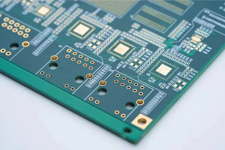
HDI PCBs are all the rage in modern electronics manufacturing. From smartphones to wearables and IoT devices, HDI PCBs are driving technological innovation and miniaturization across industries.
HDI PCBs cram a high concentration of components and interconnects into a small footprint by utilizing advanced PCB fabrication methods. This enables higher wiring densities, smaller and lighter end products, and improved electrical performance and signal integrity.
The key to unlocking the potential of HDI PCBs lies in their ability to incorporate microvias, buried vias, and blind vias. These advanced via technologies set HDI PCBs apart from standard PCBs.
Microvias are tiny vias with diameters under 150 microns that enable vertical stacking of multiple circuit layers connected by high-density interconnects. The small size allows routing tracks and vias to be placed very close to each other.
Buried vias are vias that are fabricated internally within a PCB stackup and do not connect to the outer surfaces. Blind vias are vias that connect only between internal layers and do not pass through the entire PCB.
By utilizing microvias, buried vias and blind vias in ingenious configurations, HDI PCBs achieve transformative improvements in interconnect density, signal integrity, noise isolation, and heat dissipation compared to conventional PCBs.
This article will explore how these three advanced via technologies enable HDI PCBs to deliver unmatched performance and miniaturization capabilities for today’s electronic devices.
Advanced Via Technologies for HDI PCBs
What Are Microvias?
Microvias are tiny vias with diameters under 150 microns (0.15mm) used to interconnect layers in HDI PCBs. They are much smaller than the standard vias which have diameters of 200 microns or more.
The small size of microvias allows them to be spaced very close together on HDI PCBs. This enables routing tracks and vias to be placed at a much higher density compared to conventional PCBs.
Microvias are fabricated by using advanced techniques like laser drilling and plasma etching to create tiny holes. They are then metalized to create a conductive path between the layers to be connected. Stacking microvias vertically enables connections between multiple layers.
Microvias first appeared in the 1990s and completely transformed the capability of PCBs by enabling unprecedented interconnect density. The evolution of microvias marked the birth of true HDI PCB technology.
By incorporating microvias in large numbers, HDI PCBs gained the power to integrate complex circuits with high component density and miniaturized form factors. Microvia technology opened the doors to a new generation of highly compact, high-performance electronic devices

What Are Buried Vias?
Buried vias, as the name suggests, are vias that are embedded or “buried” within the inner layers of a multilayer HDI PCB.
Unlike standard through-hole vias which span between the outermost layers, buried vias connect between internal layers without being exposed on the outer surfaces. This provides several advantages.
Firstly, buried vias isolate the signals in inner layers from interference and noise on the board’s outer surfaces. The surrounding dielectric material acts as a shield.
Secondly, buried vias improve signal integrity between inner layer circuits by providing a short and optimized conductive path. This minimizes issues like reflections and electromagnetic interference.
Thirdly, buried vias reduce crosstalk between high-speed traces in adjacent layers. The physical isolation helps prevent signal coupling.
Buried vias enable optimal routing architectures for radio frequency (RF) and high-speed digital circuits in HDI PCBs. Modern smartphones and IoT devices leverage buried vias extensively for wiring processors, memories, sensors, and communications modules.
The buried via’s shielded location and short signal path are keys to unlocking the performance potential of multilayer HDI PCBs across industries.
What Are Blind Vias?
Blind vias are vias that connect between internal layers of a multilayer HDI PCB without passing through the entire PCB stackup. Hence, they are “blind” to certain layers.
For instance, a blind via in a 6-layer PCB may connect only between layers 2 and 5 without extending to layers 1, 3, 4, and 6. This allows blind vias to conserve routing layers compared to through-hole vias.
Blind vias help optimize board layer usage in complex HDI PCBs with dozens of layers. Different connections can be segregated across layer boundaries to avoid interfering with each other.
Blind vias also enhance routing flexibility by opening up more layer-to-layer connection options. Sections of circuits can be compartmentalized across any desired layer pairs.
In wireless HDI PCBs, blind vias allow ground planes to be placed close to signals to contain electromagnetic interference. This improves signal integrity at high frequencies.
Blind and buried vias used together in complementary configurations unlock the full potential of HDI PCBs and underpin the miniaturization of modern electronics.
Advanced Vias Unlock Superior HDI PCB Performance
The ingenious use of microvias, buried vias, and blind vias in HDI PCBs confers unmatched performance capabilities that benefit next-gen electronics in multiple ways:
Higher Density Interconnects The tiny microvias act as high-speed vertical highways crisscrossing between layers in the PCB. Stacking microvias enables connectivity between circuits spread across multiple layers in 3D space without consuming much lateral real estate. The end result is an interconnect density several times higher than standard PCBs.
Signal Integrity Careful routing of traces is critical for signal integrity at high speeds. Buried vias provide short and optimized conductive paths between inner-layer circuits without external noise interference. This allows high-speed signals to propagate cleanly from their source to their destination.
Heat Dissipation Blind/buried vias dissipate heat efficiently by conducting it inwards. This allows advanced via PCBs to operate at higher power levels without overheating. The buried placement also makes the vias less disturbed by outer layer air flows that can otherwise disrupt heat conduction.
In summary, advanced vias enable HDI PCBs to simultaneously achieve miniaturization, performance, and reliability – a combination difficult to attain with legacy PCB technology.
This unique advantage makes HDI PCBs indispensable for building the powerful yet compact electronics that empower our modern world.
Advanced Vias - The Cornerstone of Modern HDI PCBs
The diminutive microvias, shielded buried vias and optimized blind vias punch far above their size class. The smart leveraging of these technologies is what unlocks the true performance potential of HDI PCBs.
By providing high-density vertical interconnects, short and isolated signal paths, and efficient heat conduction, these tiny vias enable HDI PCBs to support more components in compact spaces while enhancing electrical performance and reliability.
Whether its cramming powerful processors, abundant memory, and wireless modules into sleek smartphones or packing advanced driver assistance systems into smart cars, HDI PCBs empower the relentless march of miniaturization across consumer and industrial electronics.
As electronic devices continue to evolve and amaze, the role of HDI PCBs is only set to grow. And the advanced via a trio of microvias, buried vias, and blind vias will remain the fundamental fabrication techniques enabling HDI PCBs to fulfill demanding applications.
JHYPCB leverages these via technologies extensively in designing and producing high-performance HDI PCB prototypes as well as mid to high-volume production runs for customers worldwide.