At JHYPCB, we specialize in manufacturing and prototyping PCBs to meet the needs of our customers. As electronic devices become smaller and more complex, high-density interconnect (HDI) PCBs have become an increasingly popular option. But what exactly are HDI PCBs, and how do they differ from traditional PCBs? In this blog post, we’ll provide an overview of HDI technology and explain the key differences in design, manufacturing, performance benefits, and applications compared to standard PCBs. With our expertise in advanced PCB solutions like HDI, JHYPCB is well-positioned to help customers implement the latest circuit board innovations in their products, from smartphones and tablets to computers, automotive electronics, and cutting-edge industrial applications. Whether you need rapid prototyping or full-scale production, we have the technical knowledge and manufacturing capabilities to deliver high-quality HDI PCBs that meet your requirements.
Differences Between HDI PCBs And Traditional PCBs
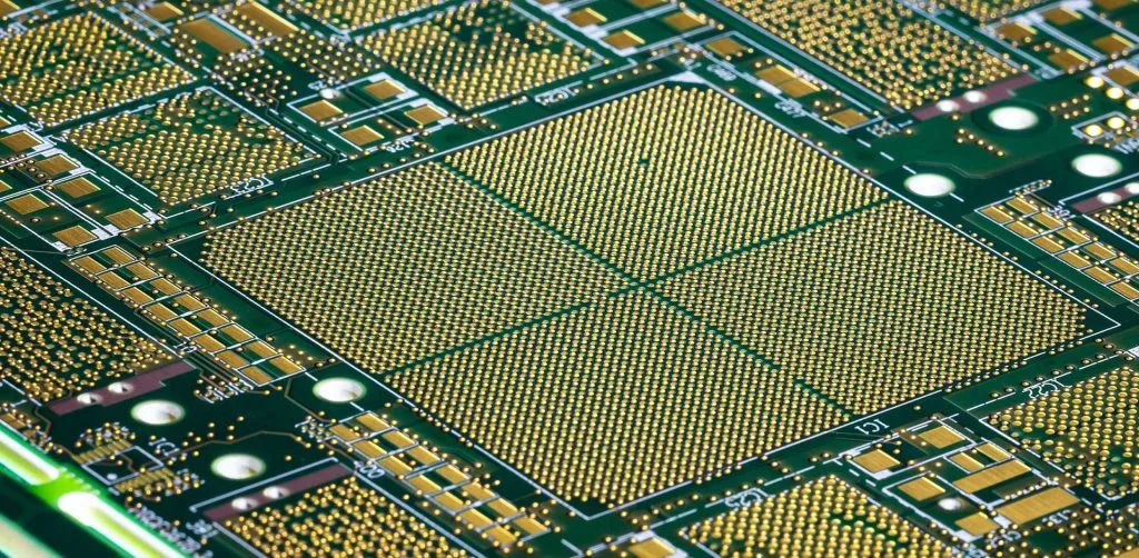
The most noticeable difference between HDI PCBs and traditional PCBs is in their construction. HDI boards are built using a technology known as the “build-up” process. This utilizes very thin laminate circuit board cores (typically 0.008” or less) along with sequentially bonded copper foil layers. The build-up process allows for extremely tight trace spacings and clearances well under 4 mils. In contrast, traditional PCBs use thicker laminate cores and pre-preg bonding sheets. They have minimum trace spacings of about 4-8 mils.
HDI PCBs also employ microvias with diameters less than 0.15 mm to interconnect layers. These microvias are laser-drilled, enabling more precision versus the mechanical drilling used for standard via holes. The combination of thin cores and microvias allows HDI PCBs to stack more circuit layers in a compact form factor. While traditional PCBs max out at around 16 layers, HDI designs can incorporate 20 layers or more within the same thickness. This is crucial for densely packed components and routing complex circuitry.
- Layer Count: HDI PCBs are a recent technology designed to increase circuit density and reduce size. One of the primary differences between HDI PCBs and traditional PCBs is the number of layers they use in construction. HDI PCBs typically have more layers than traditional PCBs, with up to 16 or more layers in some cases. The extra layers allow for higher-density components, making them ideal for compact electronic devices such as smartphones, tablets, and wearables.
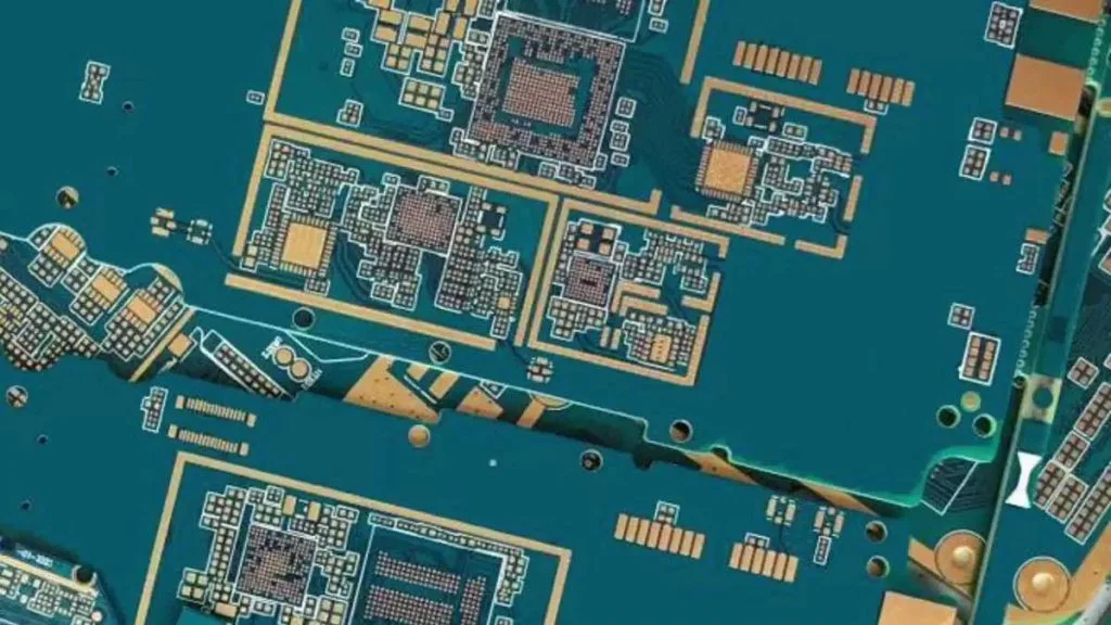
- Via Design: Another major difference between HDI PCBs and traditional PCBs is the via design. In traditional PCBs, vias are typically drilled straight through the board, which can take up a lot of space and limit component density. In contrast, HDI PCBs use smaller blind, buried, and micro vias to reduce the size and increase the density of components on the board. These techniques allow for a higher density of components on the board while also reducing the overall size of the board.
- Signal Integrity: Signal integrity is another area where HDI PCBs outperform traditional PCBs. The smaller vias used in HDI PCBs allow for shorter signal paths, reducing signal loss and interference. This is especially important in high-speed digital applications, where signal integrity is critical to the device’s proper functioning.
- Functionality: HDI PCBs also offer increased functionality over traditional PCBs. They can support various components, including Ball Grid Arrays (BGAs) and other advanced packaging technologies. This allows for more complex circuit designs and greater functionality in a smaller space.
- Complexity and Cost: However, one of the main challenges with HDI PCBs is their increased complexity, making them more difficult and expensive to manufacture. The smaller vias and higher layer counts require more advanced manufacturing techniques and specialized equipment, which can increase the cost and lead time of the PCB.
The following table summarizes the differences between HDI and traditional PCB in design, cost, functionality, and signal transmission.
| Comparison Factor | HDI PCBs | Traditional PCBs |
|---|---|---|
| Layer Count | More layers, up to 16+ | Fewer layers, typically ≤6 |
| Via Design | Smaller blind, buried, and micro vias | Mostly through-hole vias |
| Signal Integrity | Better signal integrity | Poorer signal integrity |
| Functionality | Higher functionality | Lower functionality |
| Complexity and Cost | Higher complexity and cost | Lower complexity and cost |
Benefits of HDI PCBs
The advanced construction of HDI PCBs provides several important benefits compared to standard PCB technology. First, the use of thin cores and build-up layers enables remarkable miniaturization, allowing designers to fit more components and circuitry into a small space. The laser-drilled microvias also facilitate 3D interconnectivity, embedding passive components directly into the board.
Additionally, the tightly controlled trace dimensions and layer registration result in excellent electrical performance. HDI PCBs can precisely match controlled impedance requirements for high-speed signals. They also handle high frequencies very well. The buried capacitance in the thin dielectric build-up layers helps to reduce noise.
For today’s complex and compact electronics, HDI technology delivers the integration, miniaturization, and performance enhancements that can’t be achieved with traditional PCB capabilities. This makes HDI an enabling technology for products like smartphones, IoT devices, and advanced driver-assistance automotive systems.
Challenges with HDI PCBs
While HDI PCB technology delivers significant advantages, it also comes with some challenges compared to standard PCBs. First, the HDI manufacturing process with its build-up layers and microvias is more complex. It requires advanced equipment like laser drills, which have higher capital costs. The imaging and etching of micro-scale features also demands very tight process control to prevent defects. This makes HDI PCB fabrication more expensive compared to traditional methods.
The dense packing and thin layers of HDI designs also create thermal management issues. Effective cooling is critical to prevent overheating, but the lack of airflow and close proximity of traces in HDI circuits reduces heat dissipation efficiency. Additionally, the sheer density of components makes it difficult for engineers to route out all the required interconnects. High-speed signal and power integrity verification are also essential.
Overall, reliable HDI PCB production requires significant expertise and precision manufacturing capabilities. However, the benefits outweigh the challenges for advanced electronics and mission-critical applications.
Example Applications
HDI PCB technology is ideal for advanced electronics where small size, lightweight, and high performance are critical. Some of the leading application areas include:
- Smartphones and tablets – HDI allows miniaturization and integration of processors, memories, sensors, and other components while handling high-speed data signals.
- Laptops and PCs – The high layer counts and dense interconnects of HDI facilitate powerful computing packed into thin and light consumer devices.
- Automotive electronics – The ruggedness and thermal management capabilities are beneficial in engine control units, driver assistance systems, and infotainment.
- Aerospace/defense – Reliability along with size and weight reductions make HDI suitable for guidance systems, radars, and other mission-critical uses.
- IoT devices – HDI is advantageous for the tiny integrated circuit boards needed in smart home gadgets, wearables, sensors, and more.
As electronics evolve to provide more capabilities in smaller packages, HDI PCBs will continue growing in dominance for these cutting-edge applications and beyond.
Conclusion
In summary, HDI PCB technology represents an advanced evolution compared to traditional printed circuit boards. HDI boards utilize a built-up construction with thin laminates and copper foil layers rather than thick cores and pre-preg sheets. This allows for microvias with diameters under 0.15mm to be laser drilled, providing 3D interconnectivity and component embedding.
The result is that HDI PCBs can have tighter trace spacings, smaller via sizes, and more circuit layers packed into a compact form factor. This enables increased component density and integration, improved electrical performance, and miniaturization capabilities. However, the complex HDI fabrication process does require precise process control and advanced equipment.
While traditional PCBs still work well for many applications, HDI delivers clear benefits for miniaturized, high-speed, and high-frequency electronics. With our expertise in HDI and other advanced PCB technologies, JHYPCB is ready to partner with customers to implement the latest innovations in printed circuit board design and manufacturing. Contact us today to discuss your next project!