Introduction
Printed circuit boards are the foundation of electronics. They provide the mechanical structure and electrical connections for components in devices ranging from consumer electronics to industrial equipment. As electronics become more complex and quality standards rise, effective PCB inspection is critical for ensuring the reliability and performance of electronic circuits. This article provides a comprehensive guide to the key methods used for inspecting bare PCBs and assembled PCBs (PCBAs).
Proper PCB inspection identifies defects introduced during manufacturing and assembly, preventing functional issues or field failures down the line. However, selecting the right inspection techniques can be challenging with the diversity of PCB types, components, and potential defects. By understanding available methods from visual checks to automated optical, x-ray, and flying probe inspection, PCB designers, fabricators, and assemblers can implement an inspection program that cost-effectively verifies quality requirements.
PCB inspection not only prevents shipping defective boards, but the data collected enables process improvement by identifying the root causes of issues. In light of rising quality demands and manufacturing complexity, this guide aims to equip engineering and quality control teams with the knowledge to leverage inspection at every stage – from bare boards to fully assembled PCBAs. Implementing the strategies here will reduce risks and costs while accelerating time-to-market.
Bare PCB Inspection
Bare PCB inspection focuses on verifying the quality of the bare printed circuit board before components are assembled. It identifies defects in the PCB fabrication process, which could lead to reliability issues or functionality problems in the final product. There are three main methods used:
Visual Inspection
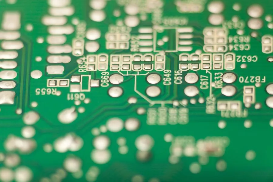
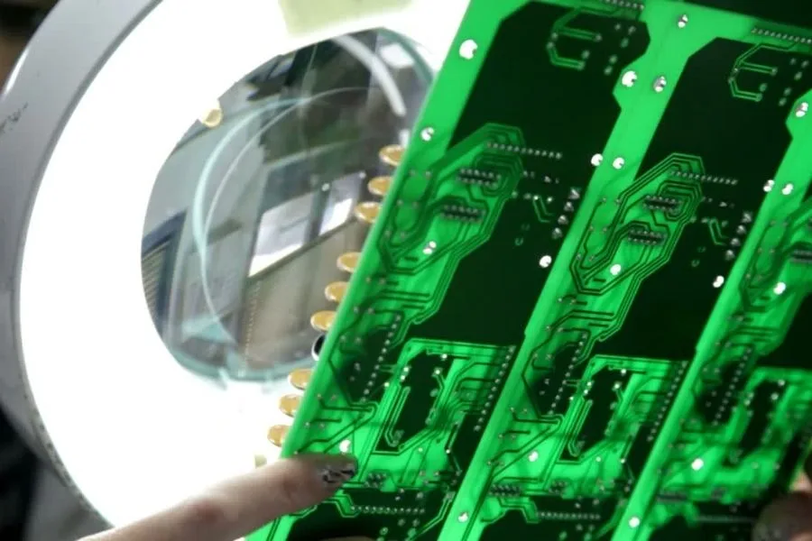
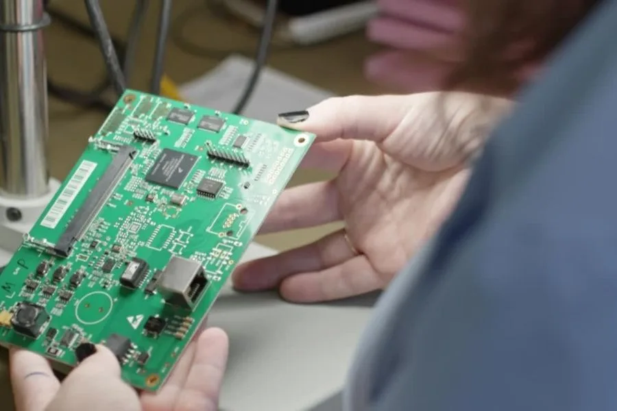
Visual inspection involves manually checking bare PCBs for any noticeable defects, damages, or irregularities. Under proper lighting and magnification, inspectors examine the PCB surfaces, edges, solder mask, silkscreen, holes, vias, traces, and other features. Visual inspection can catch obvious defects like scratches, nicks, spots, or residue. However, its effectiveness is limited by human eyesight, and minor defects may be missed.
Flying Probe Testing
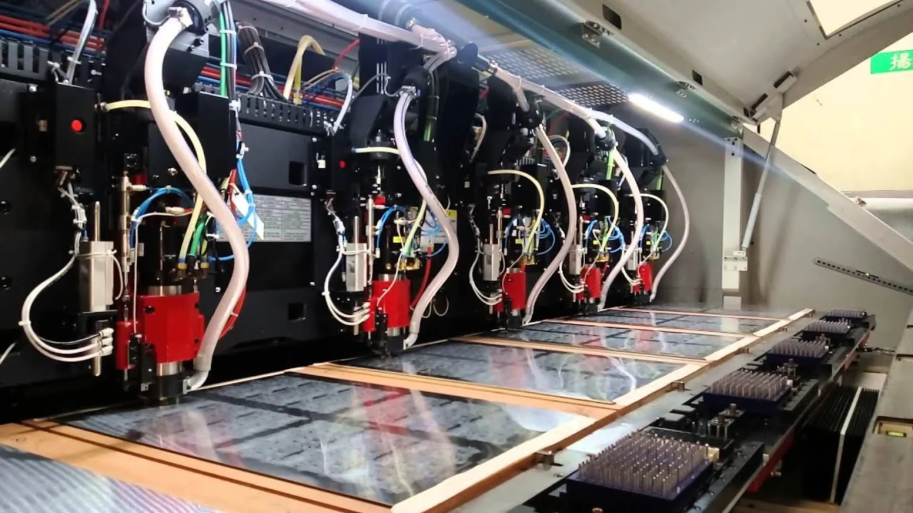
Flying probe testing uses two or four movable probes to make electrical contact and test the connectivity of traces, pads, vias, and plated through holes on a bare PCB. The flying probe tester automatically checks for short circuits or open circuits, which indicate PCB damage or faulty fabrication. Flying probe testing is very thorough since it directly verifies the electrical function of conductors on each board. However, it is slower than other inspection methods.
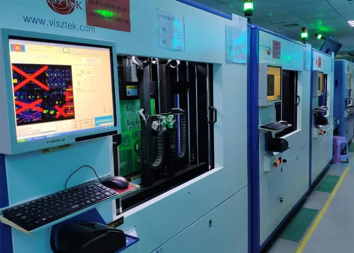
Automatic Optical Inspection (AOI)
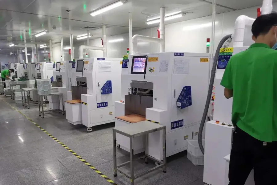
AOI systems use high-resolution cameras to capture images of a PCB surface, which are digitally processed to inspect traces, spacing, hole sizes, and other design features. The optical images are compared to an electronic CAD file to identify any discrepancies or defects. AOI inspection can find tiny flaws undetectable by visual inspection. Large-area AOI systems can quickly scan entire panels of multiple PCBs. The speed and accuracy of automated optical inspection make it the most commonly used method for verifying bare PCB quality.
Please let me know if you want me to expand or add more details on any specific inspection methods in this section.
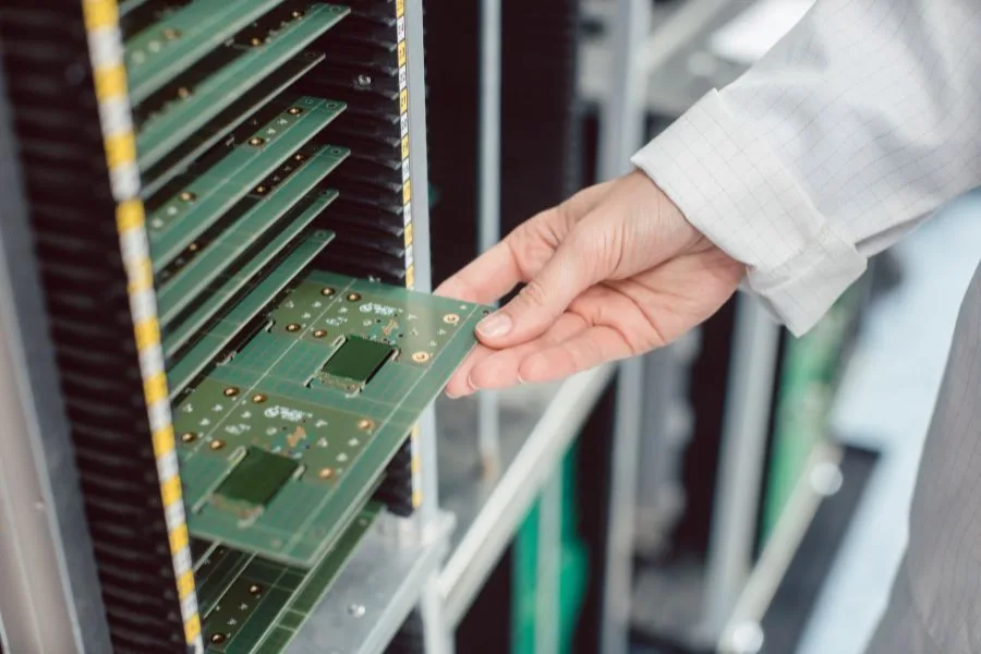
PCBA Inspection
Printed Circuit Board Assembly inspection focuses on verifying soldering quality, component placement, and assemblies on completed PCBs. Some key inspection methods include:
Component Inspection
Before assembly, all the components must be inspected to ensure they meet specifications and are free of damage. This includes checking component dimensions, leads, markings, as well as electrical performance and function. Verifying component quality reduces defects introduced in later assembly processes.
Solder Paste Inspection
Solder paste printing must be inspected prior to component placement to detect any printing defects. Typical checks include solder pad height, area coverage, and alignment to avoid faulty solder joints or bridges after reflow. Automated optical inspection and 3D SPI systems are commonly used for solder paste inspection.
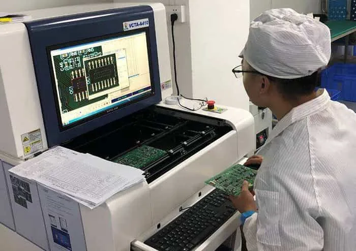
AOI Inspection
After soldering, AOI is used to check component placement and solder joints. High-resolution cameras can rapidly and accurately identify issues like missing components, misalignments, insufficient solder, shorts, or faulty connections. 3D AOI provides detailed imaging for inspection of complex solder joints.
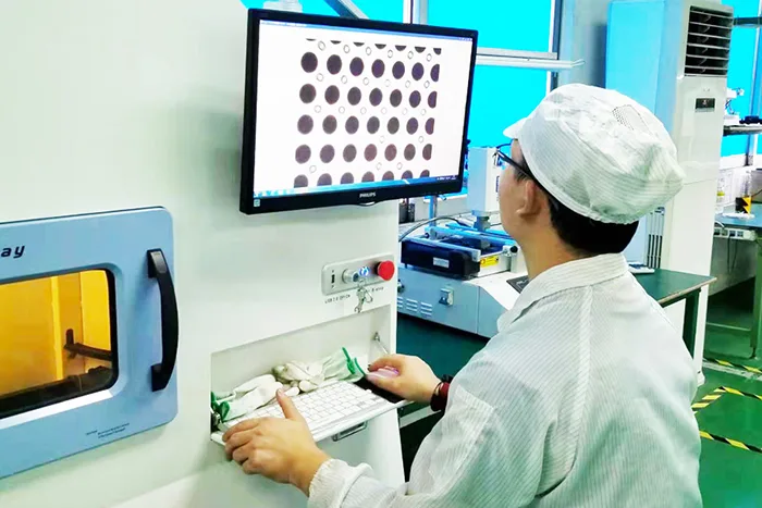
X-Ray Inspection
X-ray imaging is applied to inspect component assemblies, BGA/QFN solder joints, and internal features without disassembly. The microfocus X-ray views inside a PCB assembly allow the detection of problems like insufficient solder, voids, blown bonds, or cracks under components. X-ray inspection is very thorough but relatively slower.
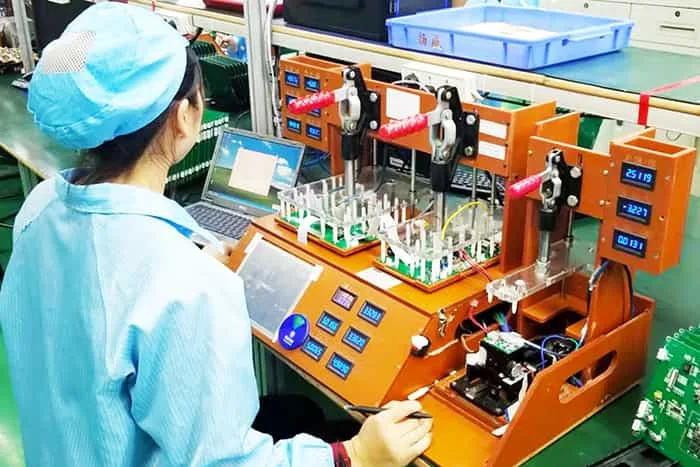
ICT (In-Circuit Testing)
In-circuit testers probe points on assembled PCBs to electrically verify connectivity, analog values, and proper functioning of each component and circuit. Dynamic ICT can test powered-up boards during operation. While slow, ICT provides direct testing of PCB assembly electronic function and performance.
Please provide feedback if you need any part of the PCBA inspection section expanded or additional methods covered.
Other Considerations
In addition to understanding available inspection techniques, implementing an effective PCB inspection program requires considering several other factors:
Inspection Sample Rate and Strategy
100% inspection may not be practical or cost-effective. An optimal sample rate must be determined based on risk, production volume, and time constraints. Critical process steps and high-value boards require higher sampling rates. Both random and targeted sampling strategies are used.
Data Management and Analytics
Modern inspection systems generate massive amounts of data. Effective software tools are essential for collecting, storing, analyzing, and reporting inspection results. Statistical analysis of inspection data also provides vital feedback to improve manufacturing processes.
Automated Handling and Integration
For high throughput, PCB inspection must be integrated with automated material handling systems like conveyors, robots, or rail-guided carts. Software interfaces between the inspection systems and manufacturing execution system enable seamless and efficient quality control workflows.
By considering these factors, PCB manufacturers can develop inspection programs tailored to their production needs and quality standards.
PCB Inspection Checklist
A PCB inspection checklist helps ensure all critical steps are covered. Here is a general checklist covering key parameters and defects to inspect for:
Bare PCB Checklist:
- Visual – Scratches, nicks, spots, residue, smears, handling damage
- Layer registration – Alignment of inner and outer layers
- Etching issues – Under/over etching, necking, pitting
- Hole quality – Barrel cracking, hole damage, plating
- Trace width/spacing – Meet design specifications
- Soldermask and silkscreen – Coverage, bleed, alignment
- Cleanliness – No debris or contamination
PCBA Checklist:
- Component defects – Damage, wrong part, misalignments
- Solder joints – Insufficient solder, shorts, opens, bridging
- PCB damage – Cracks, burns, lifted traces, delamination
- Solder balls/splatter – Prevent electrical shorts
- Flux residue – Can impede electrical connections
- Assemblies – Secured hardware, connectors, fittings
- Labelling – Correct markings and identification
Having a master inspection checklist ensures consistency and prevents overlooking any critical inspection items. Checklists can be customized for each specific PCB product and assembly process.
PCB Inspection Equipment
Implementing effective PCB inspection requires having the right equipment. Here are some common inspection systems used:
- Automated optical inspection (AOI) – High-resolution cameras and software for automated visual inspection. 3D AOI can handle complex components.
- Automated X-ray inspection – X-ray imaging systems to detect internal defects without disassembly.
- Flying probe testers – Electrically check bare PCB trace connectivity using movable probes.
- In-circuit testers (ICT) – Tests assembled PCBs by electrically probing components and circuits.
- Solder paste inspection – 3D SPI equipment to inspect print quality before soldering.
- Optical and scanning electron microscopes – High magnification visual inspection tools.
- Component counting machines – Quickly counts parts on assembled PCBs.
- PCBA programming/functional testers – Validates assembled PCB electronic functions.
Selecting the optimal inspection equipment for one’s production environment, volume, and cost considerations is key to maximizing quality and efficiency.
With this new section, the article now provides a more complete overview of key PCB inspection methods as well as the equipment needed to implement them. Please let me know if you would like me to expand or refine this section further.
Choosing the Right Inspection Approach
The choice of PCB inspection method and equipment hinges on several factors:
Production Volume: High-volume production lines benefit from automated inspection methods like AOI and ICT due to their speed and consistency. In contrast, low-volume or prototype production may rely more on manual inspection methods.
Complexity of PCB Design: PCBs come in various shapes and sizes, from simple single-layer boards to complex multilayer designs with fine-pitch components. Complex designs often necessitate advanced inspection techniques like X-ray or AOI.
Cost Considerations: The initial investment in equipment and training should align with the budget and production requirements of the project. Automated equipment can be costly, but it can offer long-term efficiency and consistency.
Regulatory Requirements: Different industries have varying levels of quality standards and regulatory requirements. For example, the aerospace and medical device industries have stringent quality requirements, necessitating specific inspection methods.
By evaluating these factors, PCB fabricators can determine the optimal combination of manual and automated inspection methods for their specific needs and budget. A balanced approach helps maximize quality while minimizing costs.
Summary
PCB inspection is a critical process in electronics manufacturing. This guide reviewed key inspection methods at both the bare PCB level and the assembled PCB level. For bare PCBs, visual inspection, flying probe testing, and automated optical inspection are commonly used to detect fabrication defects. For assembled PCBs, component inspection, solder paste inspection, automated optical inspection, x-ray imaging, and in-circuit testing are applied to verify soldering, assemblies, and functionality.
Implementing the proper inspection techniques at each manufacturing stage ensures any defects or issues are caught early before they become costly problems down the line. However, maximizing the value of inspection also requires considering additional factors like sampling strategies, data management, and integration with automation. By leveraging the various inspection methods covered here and optimizing their inspection program, PCB fabricators and assemblers can deliver superior quality products to their customers in a consistent and cost-effective manner.
As a leading PCB manufacturer in China, JHYPCB provides high-quality PCB fabrication and assembly services with 100% PCB inspection. Leveraging advanced inspection equipment and processes, JHYPCB delivers reliable, high-performance PCBs tailored to your requirements. Contact JHYPCB today to experience the quality difference of 100% inspected PCBs for your next project!
Related Reading