At the forefront of electronic innovation lies a groundbreaking technology that has revolutionized the way devices are designed and manufactured – High-Density Interconnect PCBs, or HDI PCBs. These advanced printed circuit boards have enabled a remarkable level of miniaturization and integration, paving the way for the sleek, powerful, and feature-rich electronics that have become an integral part of our daily lives.
HDI PCBs, with their intricate web of ultra-fine conductive traces and high-density interconnects, have shattered the boundaries of conventional circuit board design. By harnessing the power of microvias, buried vias, and blind vias, these ingenious boards facilitate an unparalleled density of components and circuitry within a compact footprint.
Whether you’re marveling at the stunning display and lightning-fast performance of the latest smartphone, or witnessing the seamless fusion of technology and fashion in cutting-edge wearable devices, you’re experiencing the extraordinary capabilities of HDI technology first-hand. This revolutionary approach to PCB manufacturing has become the driving force behind the relentless pursuit of smaller, faster, and more powerful electronics that continue to shape our modern world.

What is an HDI PCB?
At the core of the high-tech marvels that have reshaped our world lies a pioneering innovation – the High-Density Interconnect Printed Circuit Board, or HDI PCB. These advanced circuit boards are distinguished by their remarkable ability to pack an extraordinary density of components and interconnections into a remarkably compact footprint.
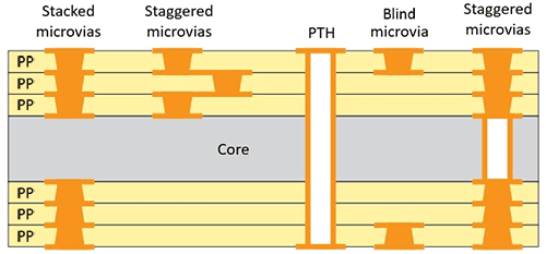
The secret to HDI PCBs’ unparalleled capabilities lies in their ingenious use of microvias, buried vias, and blind vias. These microscopic pathways, measured in mere microns, enable the dense vertical and horizontal routing of conductive traces, allowing for an intricate web of interconnections that would be impossible with conventional PCB technology.
HDI PCBs typically feature a higher layer count than their traditional counterparts, with each layer meticulously sandwiched between thin dielectric materials. This multi-layered architecture, combined with the precision of micro-vias, unlocks a whole new dimension of circuit design, enabling designers to integrate mind-boggling levels of complexity into the smallest of spaces.
From the sleek, cutting-edge 1+N+1 HDI PCBs, where a single high-density layer is encased between two standard layers, to the even more intricate 2+N+2 designs, boasting two high-density layers sandwiched between standard ones, the HDI PCB family offers a versatile range of options to meet the ever-increasing demands of modern electronics.
But the innovation doesn’t stop there. HDI PCBs can also incorporate advanced techniques such as stacked vias, staggered vias, and via-in-pad designs, each offering unique advantages and pushing the boundaries of what’s possible in high-density interconnect technology.
In an era where size and power converge, HDI PCBs have emerged as the indispensable enablers of the cutting-edge devices that have become an integral part of our daily lives. From smartphones and tablets to wearable gadgets and IoT devices, these remarkable circuit boards are the unsung heroes, quietly powering the technological revolution that continues to shape our world.

Advantages of Embracing HDI PCB Technology
As the world’s insatiable appetite for smaller, faster, and more powerful electronic devices continues to grow, High-Density Interconnect PCBs have emerged as the catalysts driving this relentless pursuit of innovation. Harnessing the power of microvias, buried vias, and ultra-fine conductive pathways, HDI PCBs offer a plethora of game-changing advantages that are propelling the electronics industry into a new era of unprecedented possibilities.
Enabling Unparalleled Miniaturization
One of the most profound advantages of HDI PCB technology is its ability to enable the remarkable miniaturization of electronic devices. By leveraging thinner dielectric layers and microscopic vias measured in mere microns, HDI PCBs allow components to be packed together with an astonishing density. While conventional PCBs typically feature trace widths and spacings in the millimeter range, HDI boards can boast traces and gaps under 100 microns – narrower than the width of a human hair!
This unparalleled compactness is the driving force behind the sleek, ultra-thin form factors of modern smartphones, tablets, and wearable gadgets, all while packing an incredible amount of computing power. Without the high-density interconnect capabilities of HDI PCBs, many of today’s svelte and portable electronics would simply not be feasible.
Accelerating Signal Speeds
In the fast-paced world of electronics, speed is paramount, and HDI PCBs deliver a significant performance boost by accelerating signal speeds. By positioning components in close proximity, HDI boards drastically reduce the distances between interconnects, minimizing signal propagation time and latency.
Whereas traditional PCBs may feature trace lengths spanning tens of millimeters, HDI designs shrink these pathways down to mere millimeters or even fractions of a millimeter. This dramatic reduction in signal travel distance translates into blazing-fast data processing speeds and responsiveness, ensuring that devices can keep pace with the ever-increasing demands of modern applications and services.
Mitigating Crosstalk and Noise Interference
In the densely packed landscape of high-frequency electronics, crosstalk and electrical noise can wreak havoc on signal integrity. As signals traverse alongside each other over significant distances, electromagnetic coupling and interference can cause distortion, data corruption, and reliability issues.
HDI PCBs elegantly mitigate these challenges by keeping conductive traces extremely short and optimally routed, minimizing the potential for crosstalk and interference. Furthermore, the ultra-thin dielectric layers separating the copper planes allow signals on different layers to coexist in close vertical proximity while remaining isolated, further reducing noise pickup and enhancing signal fidelity.
Boosting Reliability and Robustness
Beyond enabling unprecedented miniaturization and speed, HDI PCB technology also delivers a significant boost in overall system reliability. By minimizing the physical distances that signals must travel, HDI boards reduce the impact of factors like resistance, capacitance, and impedance mismatches that can degrade signal quality over longer trace lengths.
This inherent robustness ensures that signals arrive at their destinations with minimal degradation, enhancing the integrity and fidelity of data transmission. Moreover, the shorter traces facilitate heavier copper weighting, further reinforcing signal strength and resilience against interference.
Unleashing Circuit Complexity
In the ever-evolving landscape of electronics, the relentless pursuit of more advanced features and functionality drives the need for increasingly complex circuitry. HDI PCBs answer this call by enabling the integration of intricate logic and circuitry within a remarkably compact footprint.
With their ability to accommodate tens of thousands of interconnects in the same area where conventional PCBs can only manage hundreds, HDI boards empower circuit designers to pack an extraordinary level of complexity into their designs. This unparalleled density not only supports advanced system-on-chip solutions with hundreds of millions of transistors but also minimizes delays between integrated components, thanks to the ultra-short interconnect distances.
As the demands of modern electronics continue to push the boundaries of what’s possible, HDI PCB technology stands as the vanguard, enabling the seamless fusion of miniaturization, speed, reliability, and complexity that defines the cutting edge of innovation.
Conclusion
HDI PCB technology provides a number of important benefits that make it critical for modern electronics. The use of thinner dielectrics and conductive traces enables much higher component densities and interconnectivity. This allows for miniaturization and thinner profile designs that are essential for compact consumer products. HDI PCBs also improve speed and electrical performance by significantly shortening signal paths between components to just millimeters or fractions of millimeters. This reduces latency and increases data rates. Noise and crosstalk are also mitigated by the shorter traces and proper layer stacking. In addition, reliability is enhanced due to reduced signal degradation over shorter distances. Finally, the high-density interconnects facilitate the integration of much more complex circuitry. When combined, these advantages of HDI PCBs – density, speed, noise reduction, reliability, and complexity – add up to enabling the sophisticated and ever-advancing capabilities of cutting-edge electronic devices. HDI will only become more crucial as technology progresses and designs continue requiring greater functionality in smaller form factors.


