What is a Single Sided PCB?
Single-layer PCB, also known as single-sided PCB, is a type of printed circuit board that has conductive material on only one side of the substrate. Single-sided PCBs are commonly used in a variety of electronic applications due to their simplicity, low cost, and ease of manufacturing. In this article, we will provide an overview of the manufacturing process of single-layer PCBs, including design, and manufacturing.
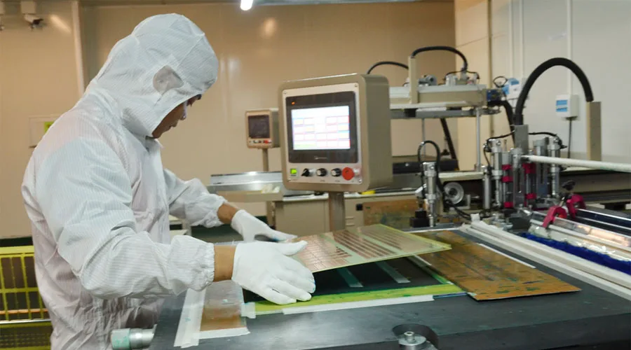
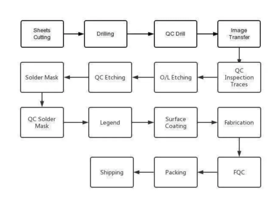
Single Sided PCB Manufacturing Process
The manufacturing process of single-layer PCBs involves several steps, including design, printing, etching, drilling, plating, and finishing. Here is a brief overview of each step:
Design – The first step in manufacturing a single-layer PCB is to create a design that specifies the location and layout of the components, traces, and pads. This design is created using specialized software that generates a digital file of the board layout.
Printing – The design file is then used to print a physical copy of the board on a special type of film or paper, known as the photomask. The photomask is used to transfer the design onto the copper layer of the PCB.
Etching – After the photomask is placed on top of the copper layer, the board is then exposed to a chemical etchant that removes the unwanted copper. This process leaves behind only the desired copper traces and pads.
Drilling – Once the copper layer is etched, the board is drilled to create holes for the components to be mounted. These holes are usually created using a computer-controlled drilling machine.
Plating – The holes are then plated with a thin layer of conductive material, such as copper or gold, to help the components make contact with the circuit.
Finishing – Finally, the board is coated with a layer of protective material, such as solder mask or silkscreen, to protect the copper traces and pads from environmental factors and provide a professional finish.
Single Layer PCB Manufacturing Techniques
In single-sided PCB manufacturing, there are several techniques that can be used to produce the desired circuit pattern on the copper-clad board. Here are some commonly used techniques:
Chemical etching: This is the most popular and widely used technique in single-sided PCB manufacturing. In this process, a resist is applied to the copper layer and a pattern is exposed through a film or photo mask. The board is then immersed in an etching solution that dissolves the exposed copper leaving behind the desired circuit pattern.
Mechanical etching: This technique uses CNC machines or other tools to physically remove the unwanted copper from the board, leaving the circuit pattern intact. Mechanical etching is more precise than chemical etching and can be used for high-precision circuits.
Screen printing: Screen printing is a process where ink is pushed through a stencil onto the copper layer. The ink resists the etching solution, leaving behind the desired pattern.
Photo-imaging: This technique is similar to chemical etching, but instead of a resist, a photosensitive film is used. The film is exposed to UV light through a film or photo mask, and the areas not exposed are developed away. The board is then etched to remove the unwanted copper.
These techniques are all used in the manufacturing of single-sided PCBs, and the choice of technique depends on the specific design and requirements of the circuit.
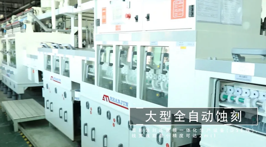
Chemical etching of PCB Manufacturing Process
Chemical etching is a popular method for manufacturing single-sided PCBs. This process involves using a chemical solution to selectively remove unwanted copper from a copper-clad board to form the desired circuit pattern. The process can be divided into several steps: cleaning, lamination, exposure, developing, and etching.
Cleaning – The first step in the chemical etching process is to clean the copper-clad board. Any contaminants on the surface of the board can interfere with the adhesion of the photoresist, making it difficult to achieve the desired circuit pattern. The board is typically cleaned with a solvent, such as acetone, and then rinsed with deionized water.
Lamination – After cleaning, a layer of photoresist is applied to the board using a process called lamination. The photoresist is a light-sensitive material that hardens when exposed to UV light. The board is placed in a vacuum laminator, and the photoresist is sandwiched between the board and a clear plastic film. The laminator applies pressure and heat to ensure that the photoresist is evenly spread across the board.
Exposure – Once the photoresist has been applied, the board is exposed to UV light through a photomask. The photomask is a film with the desired circuit pattern printed on it in black ink. When the UV light passes through the clear areas of the photomask, it hardens the photoresist underneath, leaving the unexposed areas soft.
Developing – After exposure, the board is immersed in a developer solution that dissolves the unexposed photoresist, leaving the desired circuit pattern on the board. The developer solution can be alkaline or acidic, depending on the type of photoresist used. The developer solution removes the unexposed photoresist, revealing the underlying copper.
Etching – The last step in the chemical etching process is to etch the exposed copper using an etchant solution, usually ferric chloride or ammonium persulfate. The etchant selectively dissolves the exposed copper, leaving the desired circuit pattern on the board. The etching time is carefully controlled to ensure that the desired depth of copper is removed.
After etching, the board is rinsed in water to remove any remaining photoresist and etchant. The board is then inspected for any defects and is ready for drilling and component placement.
Chemical etching is a highly precise and repeatable process that can produce complex circuit patterns with fine lines and spaces. It is suitable for both small and large production runs and is relatively inexpensive compared to other PCB manufacturing methods. However, the process requires careful handling of hazardous chemicals, and the waste products must be disposed of safely.
The Quatity Control of Single Sided PCB
There are several quality control methods that can be used for single sided PCBs. Here are some of the most common ones:
Visual Inspection: A visual inspection is one of the simplest quality control methods and can be done by the operator or inspector. The PCB is examined for defects such as scratches, cracks, misalignment, or other surface imperfections. This inspection can also identify any missing components or soldering issues.
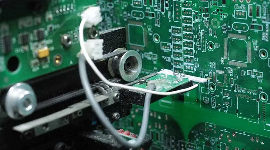
Automated Optical Inspection (AOI): An AOI system scans the PCB using cameras and checks for errors in the components, solder joints, and other defects such as missing or misplaced components. This method is highly efficient and can quickly identify and report any defects to the operator.
Electrical Testing: Electrical testing is done by applying an electrical signal to the PCB and testing for continuity and impedance. This method can detect open circuits, short circuits, and component placement errors.
X-ray Inspection: X-ray inspection can be used to check the internal structure of the PCB and components. It is especially useful for checking the placement of BGA (ball grid array) components, which are difficult to inspect visually.
Functional Testing: This method tests the PCB under real operating conditions to ensure that it works correctly. It is helpful for testing the functionality of the PCB and the components under normal usage.
These quality control methods can be used at different stages of the PCB manufacturing process. For example, visual inspection can be done during the printing and etching process to ensure the board is free of defects. Electrical testing can be done after component placement and soldering to ensure that the components are correctly placed and soldered. Finally, functional testing is done after the final assembly of the PCB to ensure it is fully functional.
By implementing quality control methods, manufacturers can ensure that single-sided PCBs meet high-quality standards and are free of defects. This ensures that the PCBs function correctly and are reliable, which is essential for electronic devices.
What are the Advantages and Disadvantages of Single Layer PCB?
Single sided PCBs have both advantages and disadvantages in their manufacturing process. Let’s take a closer look at them:
Advantages:
Cost-effective: Single sided PCBs are the most cost-effective option for low-complexity circuits, making them a popular choice for simple electronic devices. Their simple design and manufacturing process make them easy to produce in large quantities, which can result in lower per-unit costs.
Easy to design and manufacture: Single sided PCBs are simple to design and manufacture, making them a good choice for small-scale production or for hobbyists. This also makes them easy to repair and modify if necessary.
Simple assembly: With only one layer of components, single-layer PCBs are easier to assemble than multi-layer PCBs. This can save time and effort during the manufacturing process.
Space-saving: Single-sided PCBs are thinner and take up less space than multi-layer PCBs, making them a good choice for compact electronic devices. This can be an advantage in applications where space is at a premium.
Lower signal interference: Single-sided PCBs have less signal interference compared to multi-layer PCBs, as they do not have multiple ground planes or signal traces interfering with each other.
Disadvantages:
Limited complexity: Single-sided PCBs are limited in their complexity, making them unsuitable for complex circuits or advanced electronic devices. Their simple design means they cannot accommodate many components or complex routing.
Larger size: Due to the limited number of layers, single-layer PCBs tend to be larger in size compared to multi-layer PCBs, which can be a disadvantage for devices where space is at a premium.
Signal interference: Although single-sided PCBs have lower signal interference compared to multi-layer PCBs, they are still prone to interference due to the lack of a separate ground plane. This can impact performance, especially in applications where signal integrity is critical.
Reduced functionality: Single-sided PCBs have limited functionality compared to multi-layer PCBs, which can limit their use in more advanced devices. They may not be able to handle high-speed signals or complex circuits.
More prone to errors: Single-sided PCBs require careful layout and design to ensure that all components are correctly placed and the circuit functions properly, making them more prone to errors during the manufacturing process. This can result in a higher defect rate and increased costs.
Conclusion
Single-layer PCBs are a simple, cost-effective, and widely used technology in the electronics industry. Understanding the manufacturing process of single-layer PCBs is essential for anyone interested in designing and building electronic circuits. With the right tools and techniques, it is possible to create reliable and high-quality single-layer PCBs that meet the specific needs of your electronic projects.
Looking for a reliable and high-quality PCB manufacturer? Look no further! At JHYPCB, we offer state-of-the-art PCB manufacturing services with a team of experienced professionals and cutting-edge technology. Whether you need single-layer, multi-layer, or flexible PCBs, we have the expertise and resources to deliver on your needs. Contact us today to discuss your requirements and receive a free quote!
Related Reading:
- A Guide to Multilayer PCB Manufacturing Process
- The Ultimate Guide to Aluminum PCB Manufacturing Process
- A Comprehensive Guide to Rigid Flex PCB Fabrication & Manufacturing Process
- Reliability and Stability of Rigid PCBs: Testing and Optimization Methods
- Metal Core PCB Manufacturing Process Step by Step
- The Specialized Manufacturing Process for Heavy Copper PCBs
- Key Considerations for Choosing a Reliable Single-Layer PCB Manufacturer
- How To Tell single layer PCB From double-sided PCB?
- What is a printed circuit board (PCB)?
- What are the Single Layer PCB Types?
- V-Cut Scoring: An Essential Technique for PCB Fabrication
- PCB Profiling – Cutting Methods and Their Effects on PCB Quality
- PCB Gerber Files – Everything You Need to Know
- Building High Quality PCBs – A Comprehensive Guide