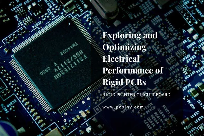
Rigid Printed Circuit Boards (Rigid PCBs) are the foundation of modern electronics, providing a stable and durable base for mounting and interconnecting electronic components. As critical components in a wide range of devices, from computers and medical equipment to automotive systems, the reliability and stability of rigid PCBs are paramount. Even the slightest defect or failure can compromise the performance and longevity of the entire electronic system.
This article delves into the crucial aspects of ensuring the reliability and stability of rigid PCBs throughout their lifecycle, from design and manufacturing to rigorous testing and optimization methods. We will explore proven techniques for evaluating the performance of rigid PCBs under various environmental, mechanical, and electrical conditions, as well as strategies for optimizing material selection, design considerations, and manufacturing processes.
By understanding and implementing best practices for rigid PCB reliability testing and optimization, manufacturers can deliver high-quality, long-lasting products that meet or exceed industry standards and customer expectations. Whether you are a PCB designer, PCB manufacturer, or anyone invested in the electronics industry, this comprehensive guide will provide valuable insights into achieving superior rigid PCB performance and stability.
What is a Rigid PCB?
A rigid printed circuit board is a type of PCB that features a solid, inflexible base material. Unlike their flexible counterparts, rigid PCBs are designed to maintain their shape and structural integrity even under various environmental and mechanical stresses.
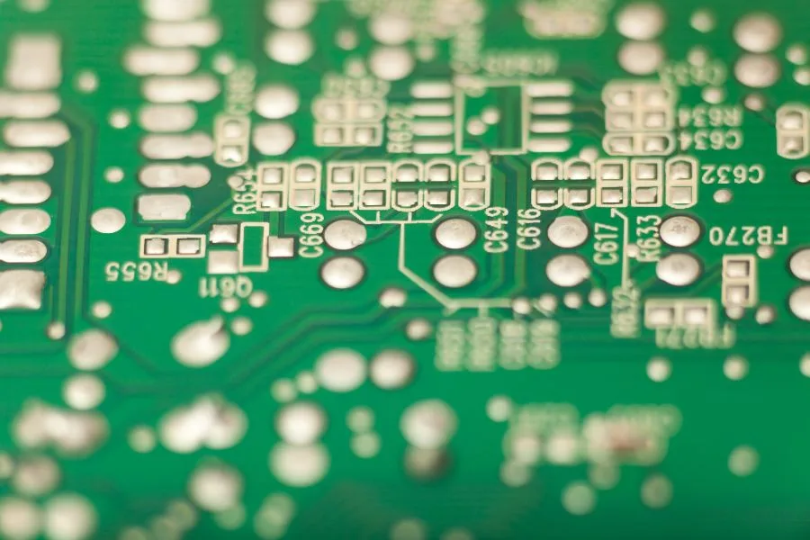
The core of a rigid PCB is typically made from a sturdy substrate like FR-4, a glass-reinforced epoxy laminate known for its excellent dielectric properties and mechanical strength. One or both sides of this substrate are layered with a conductive copper foil, which is then etched away to create the desired circuit patterns.
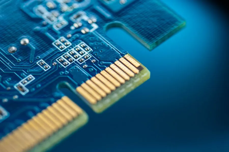
Rigid PCBs come in single-sided, double-sided, and multi-layer configurations, with the layers connected through mechanically drilled holes called vias. These robust boards offer superior rigidity, dimensional stability, and resistance to warping or deformation, making them ideal for applications that require a high degree of reliability and durability.
From basic consumer electronics to complex industrial machinery, rigid PCBs are ubiquitous in modern technology. Their stable platform enables the secure mounting of a diverse array of electronic components, including processors, memory chips, capacitors, resistors, and intricate interconnections. This solid foundation is crucial for ensuring the proper functioning and longevity of the electronic device.
With their rugged construction and ability to withstand harsh environments, rigid PCBs have become an indispensable component in a wide range of industries, including aerospace, automotive, medical, telecommunications, and more. As technology continues to advance, the demand for reliable and high-performance rigid PCBs will only continue to grow.

Reliability Testing Methods for Rigid PCBs
1. Environmental Testing
To ensure optimal performance and longevity, rigid PCBs must undergo a series of rigorous environmental tests that simulate the harsh conditions they may encounter during their lifecycle. These tests evaluate the PCB’s resistance to factors such as extreme temperatures, humidity, and chemical exposure, which can potentially compromise its structural integrity and electrical performance.
High Accelerated Temperature and Humidity Stress Testing (HAST)
High Accelerated Temperature and Humidity Stress Testing (HAST) is one of the most critical environmental tests for rigid PCBs. This test evaluates the PCB’s ability to withstand prolonged exposure to high temperatures and humidity levels, accelerating the effects of these conditions on the board’s materials and components.
During HAST, the rigid PCB is placed in a pressure chamber and subjected to temperatures typically ranging from 110°C to 130°C (230°F to 266°F) and relative humidity levels of 85% or higher. These extreme conditions can reveal potential weaknesses in the PCB’s design, materials, or manufacturing processes, such as delamination, corrosion, or electrical failures.
HAST is particularly valuable for identifying issues related to moisture ingress, which can lead to ionic contamination, electrical shorts, and other reliability problems. By subjecting the PCB to accelerated aging, manufacturers can evaluate its long-term performance and make necessary adjustments to improve its durability.
Real-world Example: A leading manufacturer of medical devices discovered that their rigid PCBs were failing prematurely due to delamination issues. After conducting HAST, they identified that the specific combination of materials used in their PCB design was susceptible to moisture ingress at high temperatures and humidity levels. By optimizing their material selection and implementing design modifications, they were able to significantly enhance the reliability of their PCBs, ensuring patient safety and reducing costly product recalls.
Temperature Cycling Testing
Temperature cycling is another critical environmental testing method that evaluates the rigid PCB’s ability to withstand repeated exposure to extreme temperature variations. This test simulates the thermal stresses that PCBs may encounter in real-world applications, such as outdoor electronics, automotive systems, or aerospace components.
During temperature cycling testing, the rigid PCB is subjected to a series of alternating high and low-temperature cycles within a controlled environmental chamber. Typical temperature ranges can vary from -55°C (-67°F) to 125°C (257°F) or even wider, depending on the specific application and industry standards.
The rapid temperature fluctuations cause the PCB materials and components to expand and contract, putting stress on solder joints, interconnections, and the board itself. This thermal cycling can reveal potential weaknesses, such as cracks, delamination, or open circuits, which may lead to electrical failures or reduced performance over time.
One of the key advantages of temperature cycling testing is its ability to accelerate the aging process of the PCB, allowing manufacturers to evaluate its long-term durability in a relatively short period. By subjecting the board to hundreds or even thousands of thermal cycles, potential issues can be identified and addressed before the product reaches the market.
Real-world Example: An automotive electronics manufacturer was experiencing intermittent failures in their rigid PCBs used in engine control units. After conducting temperature cycling tests, they discovered that the solder joints were cracking due to the repeated thermal expansions and contractions experienced in the harsh under-hood environment. By optimizing the solder paste composition and reflow profile, they were able to improve the solder joint integrity, significantly enhancing the reliability of their PCBs in automotive applications.
Temperature cycling testing is often combined with other environmental tests, such as vibration or humidity exposure, to simulate real-world conditions more accurately and identify potential failure modes more comprehensively.
Salt Spray Testing
In many applications, rigid PCBs are exposed to harsh environments where corrosion can be a significant concern. Salt spray testing is a crucial environmental evaluation that assesses the PCB’s resistance to corrosive atmospheres, particularly those containing salt or other chloride-based compounds.
During salt spray testing, the rigid PCB is placed in an enclosed chamber and subjected to a constant spray of salt solution, typically a 5% sodium chloride (NaCl) solution. This solution simulates the corrosive effects of marine or coastal environments, as well as certain industrial settings where chloride-based chemicals are present.
The salt spray test is conducted over an extended period, often ranging from a few hours to several weeks, depending on the specific industry standards and requirements. The duration and severity of the test are designed to accelerate the corrosion process and reveal any potential weaknesses in the PCB’s materials, coatings, or design.
As the salt spray continues, any unprotected metallic surfaces on the PCB, such as copper traces, solder joints, or exposed components, can begin to corrode and degrade. This corrosion can lead to electrical failures, reduced conductivity, or even complete loss of functionality if left unchecked.
Real-world Example: A manufacturer of telecommunications equipment experienced frequent failures in their rigid PCBs installed in coastal regions. After conducting salt spray testing, they discovered that the conformal coating used on their PCBs was inadequate in protecting against the corrosive marine environment. By switching to a more robust conformal coating material and optimizing the application process, they were able to significantly improve the corrosion resistance of their PCBs, ensuring reliable performance in even the harshest coastal conditions.
Salt spray testing is particularly crucial for rigid PCBs intended for use in marine, automotive, offshore, or industrial environments where corrosion is a major concern. By identifying and addressing potential corrosion issues early in the design and manufacturing process, manufacturers can improve the long-term reliability and longevity of their PCBs.
2. Mechanical Testing
In addition to withstanding environmental stresses, rigid PCBs must also demonstrate robust mechanical performance to ensure reliable operation in various applications. Mechanical testing evaluates the PCB’s ability to withstand physical forces such as vibration, shock, and mechanical stress, which can potentially lead to failures like cracks, delamination, or component dislodgement.
Vibration Testing
Vibration is a common mechanical stress that rigid PCBs often encounter, particularly in applications such as automotive, aerospace, or industrial machinery. Vibration testing subjects the PCB to controlled vibrations of varying frequencies and amplitudes, simulating the conditions it may face during operation or transportation.
During vibration testing, the rigid PCB is securely mounted on a vibration table or fixture, which generates precise vibration profiles along different axes (e.g., X, Y, Z). The vibration levels and frequencies are carefully controlled to match the specific application requirements or industry standards.
This testing aims to identify potential weaknesses in the PCB’s design, materials, or component mounting that could lead to issues such as solder joint fatigue, trace cracking, or component dislodgement. Prolonged exposure to vibration can also cause gradual degradation of the PCB’s integrity, potentially leading to intermittent failures or reduced performance over time.
Real-world Example: A manufacturer of industrial automation equipment experienced recurring failures in their rigid PCBs due to solder joint cracks. After conducting extensive vibration testing, they discovered that the specific vibration profile encountered in their machinery was causing excessive stress on the solder joints. By optimizing the PCB layout, component placement, and solder joint design, they were able to significantly improve the vibration resistance of their PCBs, ensuring reliable operation in demanding industrial environments.
Shock Testing
While vibration testing evaluates the PCB’s performance under continuous mechanical stress, shock testing assesses its ability to withstand sudden, high-impact forces. These forces can occur during transportation, handling, or in applications where the PCB may be subjected to abrupt mechanical shocks, such as in automotive collisions or dropped devices.
In shock testing, the rigid PCB is subjected to controlled, high-acceleration impacts along various axes. These impacts can range from relatively mild to extremely severe, depending on the specific application requirements and industry standards.
The goal of shock testing is to identify any potential failures or damage caused by the sudden mechanical forces, such as cracked components, broken solder joints, delamination, or structural damage to the PCB itself. Even a single high-impact shock can potentially compromise the PCB’s integrity and lead to immediate or long-term reliability issues.
Real-world Example: A leading manufacturer of ruggedized handheld devices discovered that their rigid PCBs were failing when the devices were accidentally dropped. Through shock testing, they identified that the specific mounting design and component placement on the PCB were susceptible to damage from high-impact shocks. By optimizing the PCB layout, implementing additional support structures, and carefully selecting shock-resistant components, they were able to significantly improve the drop resistance of their handheld devices, ensuring reliable performance even in harsh field conditions.
Mechanical testing, encompassing vibration and shock evaluations, is crucial for ensuring the long-term reliability and durability of rigid PCBs in a wide range of applications where they are subjected to physical stresses and demanding operating environments.
3. Electrical Performance Testing
In addition to environmental and mechanical stresses, rigid PCBs must also meet stringent electrical performance requirements to ensure proper functionality and reliability. Electrical performance testing evaluates the PCB’s electrical characteristics, such as conductivity, insulation resistance, and signal integrity, under various operating conditions.
Electrical Performance Measurement
Electrical performance measurement is a comprehensive testing process that assesses the PCB’s ability to transmit signals and power efficiently and accurately. This testing typically involves subjecting the PCB to a range of electrical loads, frequencies, and conditions while measuring key performance parameters.
Some of the critical electrical performance measurements for rigid PCBs include:
- Insulation Resistance: Measures the resistance between conductive traces or layers to ensure proper insulation and prevent short circuits or leakage currents.
- Continuity Testing: Verifies the integrity of conductive paths and traces, ensuring proper electrical connectivity throughout the PCB.
- Signal Integrity: Evaluates the PCB’s ability to transmit high-frequency signals without distortion, attenuation, or interference, which is crucial for high-speed digital and RF applications.
- Power Integrity: Assesses the PCB’s capability to deliver stable and consistent power to components, preventing voltage drops, noise, or other power delivery issues.
These tests are typically performed using specialized test equipment, such as LCR meters, network analyzers, or signal integrity testers, depending on the specific measurement requirements.
Real-world Example: A manufacturer of high-speed telecommunications equipment was experiencing signal integrity issues in their rigid PCBs, leading to data errors and reduced performance. Through comprehensive electrical performance testing, they identified that the PCB layout and trace routing were causing excessive crosstalk and signal reflections. By optimizing the PCB design, implementing impedance control techniques, and utilizing advanced signal integrity simulations, they were able to significantly improve the signal quality and reliability of their PCBs, ensuring optimal data transmission rates.
Short Circuit and Open Circuit
Check In addition to performance measurements, electrical testing also includes critical checks for short circuits and open circuits, which can render the PCB inoperable or cause potential safety hazards.
Short circuit testing involves applying a voltage or current source to the PCB and measuring the resistance between conductive paths or layers that should be isolated. Any abnormally low resistance values indicate a short circuit, which can cause excessive current flow, overheating, or even fire hazards.
Open circuit testing, on the other hand, verifies the continuity of conductive paths and traces by measuring the resistance or applying a signal. Any abnormally high resistance or lack of signal transmission indicates an open circuit, which can prevent proper operation or cause intermittent failures.
These tests are typically performed using specialized testing equipment, such as continuity testers, resistance meters, or in-circuit testers, depending on the complexity of the PCB and the required test coverage.
Real-world Example: A medical device manufacturer experienced intermittent failures in their rigid PCBs used in critical life-support equipment. Through rigorous open circuit testing, they identified that certain solder joints were developing cracks over time, leading to intermittent open circuits. By optimizing the soldering process, implementing stricter quality control measures, and incorporating redundant circuit paths, they were able to significantly improve the reliability of their PCBs, ensuring continuous and safe operation of their life-saving medical devices.
Electrical performance testing is a crucial step in the development and manufacturing of rigid PCBs, as it ensures that the boards meet the required electrical specifications and operate reliably under various conditions, preventing potential failures, signal integrity issues, or safety hazards.

Optimization Methods for Rigid PCB Reliability
1. Material Selection
Selecting the right materials is a critical step in optimizing the reliability of rigid PCBs. The choice of materials can significantly impact the board’s performance, durability, and resistance to various environmental and mechanical stresses. Here are the key considerations for material selection:
Base Material (Substrate): The base material, or substrate, forms the foundation of the rigid PCB and plays a crucial role in its overall stability and performance. Common substrate materials include FR-4, polyimide, ceramic, and metal-core PCBs. Each material has its unique properties, such as dielectric constant, thermal conductivity, and coefficient of thermal expansion (CTE). The selection of the substrate should be based on the specific application requirements, such as operating temperature range, frequency characteristics, and mechanical stress levels.
Copper Foil: Copper foil is the conductive layer that forms the traces and pads on the PCB. Factors to consider when selecting copper foil include thickness, surface treatment (e.g., electroless nickel immersion gold), and roughness. Thicker copper foils provide higher current-carrying capacity and better heat dissipation, while surface treatments can enhance solderability and protect against oxidation.
Solder Mask and Conformal Coatings: Solder masks and conformal coatings provide insulation and protection for the PCB. Solder masks prevent solder bridging and ensure proper component placement, while conformal coatings protect against moisture, chemicals, and environmental contaminants. The selection of these materials should consider factors such as temperature resistance, chemical compatibility, and electrical properties.
Reinforcement Materials: Reinforcement materials, such as fiberglass or aramid fibers, can be incorporated into the PCB substrate to enhance mechanical strength and dimensional stability. These materials can improve the PCB’s resistance to warping, cracking, and delamination, especially in applications with high vibration or thermal cycling.
Careful consideration of material properties, compatibility, and application requirements is crucial for optimizing the reliability of rigid PCBs. Manufacturers should work closely with material suppliers and conduct thorough testing to ensure the selected materials meet the desired performance and reliability standards.
2. Design Considerations
Optimizing the design of rigid PCBs is essential for achieving reliable and stable performance. Proper design considerations can mitigate potential failure modes, enhance signal integrity, and improve overall board durability. Here are some key design considerations for optimizing rigid PCB reliability:
Circuit Layout: The circuit layout plays a crucial role in ensuring signal integrity, power distribution, and thermal management. Careful attention should be given to trace routing, component placement, and layer stack-up to minimize crosstalk, electromagnetic interference (EMI), and impedance mismatches. Advanced simulation tools and design rules can aid in optimizing the layout for high-frequency and high-speed applications.
Component Placement and Clearances: Proper component placement and clearances are essential for mechanical stability and thermal management. Components should be positioned to minimize stress concentrations, particularly for components with different coefficients of thermal expansion (CTE). Adequate clearances should be maintained between components and board edges to prevent potential short circuits or mechanical interference.
Thermal Management: Thermal management is a critical aspect of PCB design, especially for high-power applications. Incorporating thermal vias, heat sinks, and proper copper distribution can effectively dissipate heat and prevent hotspots, which can lead to component failure or warping of the PCB.
Mechanical Reinforcement: Depending on the application, mechanical reinforcement techniques may be necessary to enhance the rigid PCB’s structural integrity. These can include the use of stiffeners, mounting holes, or additional layers of reinforcing materials such as aramid fibers or metal cores.
Design for Testability and Rework: Incorporating design features that facilitate testing and rework can improve the overall reliability and maintainability of the PCB. This includes providing test points, allowing access for probing and inspection, and designing for easy component replacement or repair.
By considering these design factors and leveraging advanced simulation and analysis tools, PCB designers can optimize the rigid PCB’s layout, component placement, and overall construction to ensure reliable performance and mitigate potential failure modes.
3. Manufacturing and Assembly Processes
The manufacturing and assembly processes employed for rigid PCBs play a crucial role in ensuring their reliability and stability. Optimized processes can minimize defects, improve quality, and enhance the overall performance of the PCBs. Here are some key considerations for optimizing manufacturing and assembly processes:
Surface Mount Technology (SMT): Surface Mount Technology (SMT) is the predominant method for assembling rigid PCBs, offering high component density and miniaturization. Optimizing SMT processes, such as solder paste printing, component placement accuracy, and reflow soldering profiles, can significantly improve solder joint quality and reduce defects like tombstoning, poor wetting, or voiding.
Reflow Soldering: Reflow soldering is a critical step in the SMT process, where the PCB and components are exposed to high temperatures to melt the solder paste and form reliable interconnections. Optimizing reflow soldering parameters, such as temperature profiles, conveyor speed, and atmosphere control, can enhance solder joint integrity, minimize thermal stress, and prevent issues like tombstoning or component shifting.
Automated Optical Inspection (AOI): Incorporating Automated Optical Inspection (AOI) systems in the manufacturing process can significantly improve quality control and defect detection. AOI systems can identify issues such as solder defects, component misalignment, and missing or incorrect components, allowing for timely corrective actions and reducing the risk of defective PCBs reaching the market.
Cleanroom Environment: Maintaining a controlled cleanroom environment during PCB manufacturing can minimize contamination from particles, moisture, and other environmental factors that can compromise the reliability of the final product. Appropriate cleanroom classifications, air filtration systems, and strict process controls are essential for ensuring consistent quality.
Process Monitoring and Control: Implementing robust process monitoring and control systems can help maintain consistent quality and identify potential issues before they escalate. This includes monitoring parameters such as temperature, humidity, and equipment calibration, as well as implementing statistical process control (SPC) techniques to ensure processes remain within specified limits.
By optimizing manufacturing and assembly processes, PCB manufacturers can minimize defects, improve yield, and enhance the overall reliability and stability of their rigid PCBs, ultimately delivering high-quality products that meet or exceed customer expectations.
Conclusion
In conclusion, the reliability and stability of rigid PCBs are critical factors that must be taken into account during the design, manufacturing, and testing stages. Several tests and optimization methods can be used to ensure that the PCBs meet industry standards and perform reliably under different environmental, mechanical, and electrical conditions. By carefully selecting materials, considering design factors, and using appropriate manufacturing and assembly methods, designers and manufacturers can optimize the reliability and stability of rigid PCBs and ensure the long-term performance of electronic devices.
Related Reading