
PCB Knowlege
What are the Different Types of Flexible Circuits?
From single-sided to sculptured circuits, explore the various types of flexible PCBs and their unique features, advantages, and applications in this comprehensive guide.
From single-sided to sculptured circuits, explore the various types of flexible PCBs and their unique features, advantages, and applications in this comprehensive guide.

The versatility of flex circuits lies in their ability to offer unique advantages such as flexibility, lightweight, compact design, and improved reliability, making them ideal

Flex circuits, also known as flexible printed circuits or FPCs, are specialized electronic interconnects that are constructed using flexible materials.

Flexible PCBs have several advantages over rigid PCBs. However, like any other technology, flexible PCBs also have their disadvantages.
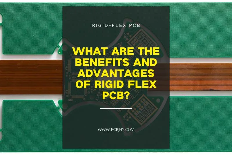
With the increasing demand for high-performance and miniaturized electronic devices in today’s market, rigid-flex PCBs have become increasingly popular. In this article, we will explore

Whether you’re a seasoned electronics professional or just starting out in the field, understanding the materials that make up Rigid-Flex PCBs is essential for designing

This article aims to introduce the factors that affect the manufacturing cost of rigid-flex PCB and how to reduce its cost.

Designing rigid-flex PCBs can be challenging, as it requires careful consideration of factors such as materials, layer stackup, trace width and spacing, and component placement.
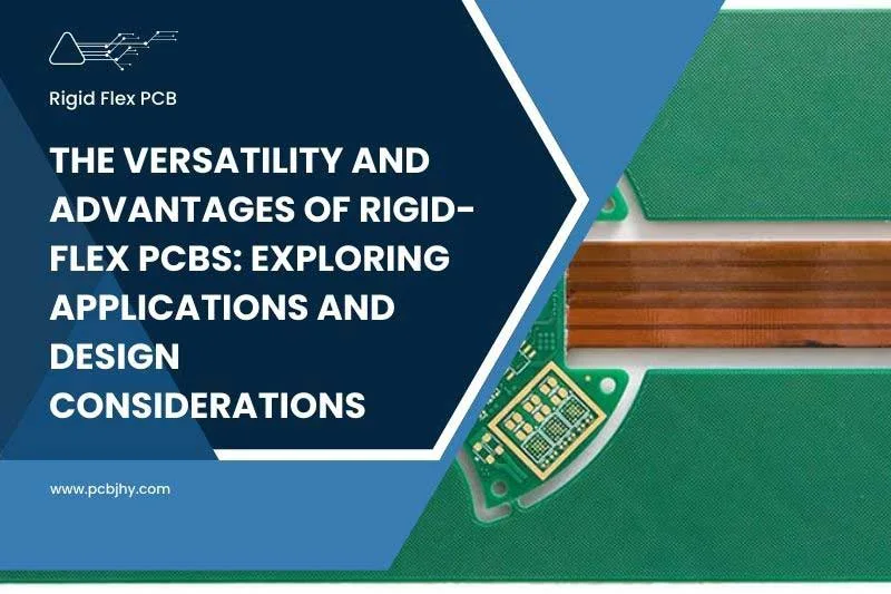
Rigid-flex PCBs have become increasingly popular due to their ability to reduce space requirements and increase reliability in complex electronic devices.

In this article, we will discuss the reliability and stability of rigid PCBs, and explore testing and optimization methods to ensure they meet industry standards.