Flex PCB Assembly Services
Professional flexible circuit assembly for single-sided, double-sided, multilayer, and rigid-flex PCBs. SMT and THT on polyimide with carrier fixturing, stiffener bonding, and 100% AOI inspection.
What Is Flex PCB Assembly?
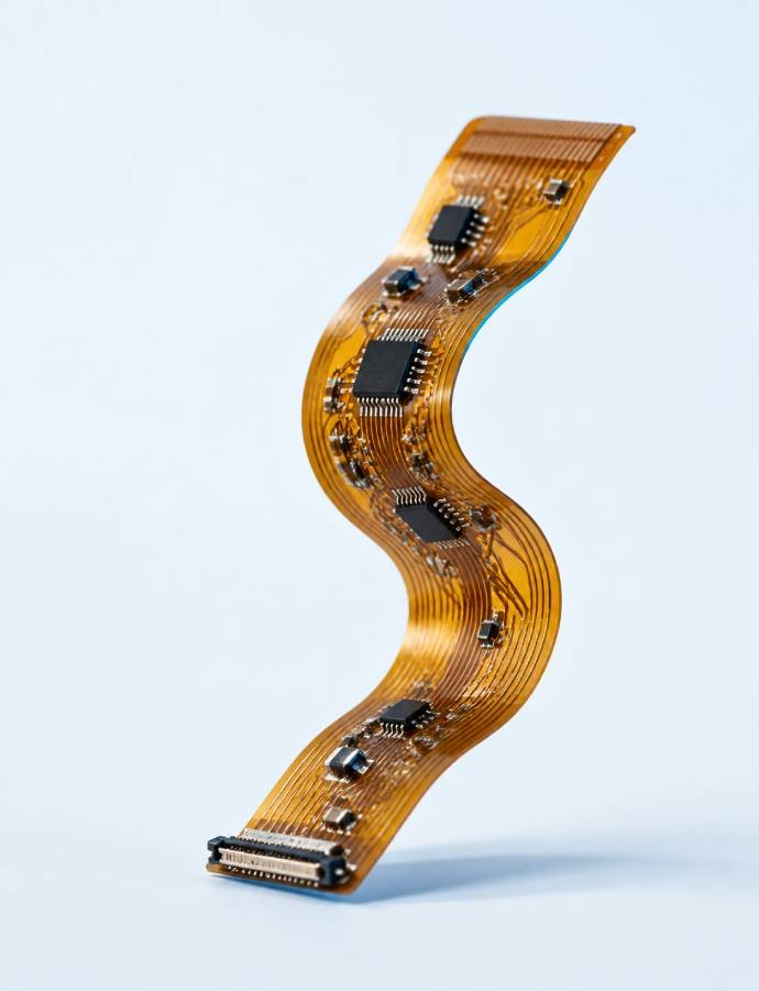
Flex PCB assembly is the process of mounting electronic components onto flexible printed circuits built from polyimide film. Unlike rigid PCB assembly, it requires high-temperature carriers for panel support, adhesive-backed stiffeners beneath component zones, and coverlay in place of solder mask. Components are attached using SMT and through-hole processes adapted for flexible substrates.
Flexible circuits bend, fold, and twist during use, enabling 3D packaging in wearables, medical devices, and automotive camera modules. Assembling components on these circuits demands specialized fixturing, modified reflow profiles, and strict bend-zone rules to protect copper traces from fatigue cracking.

Flexible Circuit Types We Assemble
JHYPCB assembles all four flexible circuit construction types, from single-layer sensor circuits to high-layer-count rigid-flex boards.
| Circuit Type | Layer Count | Typical Applications | Assembly Notes |
|---|---|---|---|
| Single-Sided Flex | 1 | Sensor connections, LED strips, battery packs | Lightest construction; supports dynamic bending with RA copper |
| Double-Sided Flex | 2 | Compact interconnects, display modules | Plated through-holes; stiffer — static bends only |
| Multilayer Flex | 3–6 | High-density signal routing, impedance control | Stiffeners required at component zones; controlled impedance available |
| Rigid-Flex | 2–20 | Aerospace harnesses, medical probes, camera modules | Rigid islands carry components; flex sections replace connectors |
Not sure which construction fits your application? Send us your drawing — our engineers recommend the most cost-effective circuit type and stiffener plan.
Our Flex PCB Assembly Process
Every flex circuit assembly follows a controlled six-step process engineered for polyimide substrates, with first-pass yield protected by carrier fixturing and full inspection.
-
1. Panel & Carrier Preparation
— Flex circuits arrive in panels or as single pieces. Each is fixed to a high-temperature carrier (aluminum or carbon fiber) using high-temp tape, magnetic clamping, or vacuum fixturing, providing rigid support through printing and reflow. -
2. Solder Paste Printing
— Paste is printed on the carrier-supported panel using laser-cut stencils. 3D SPI (Solder Paste Inspection) verifies paste volume on every flex pad before placement. -
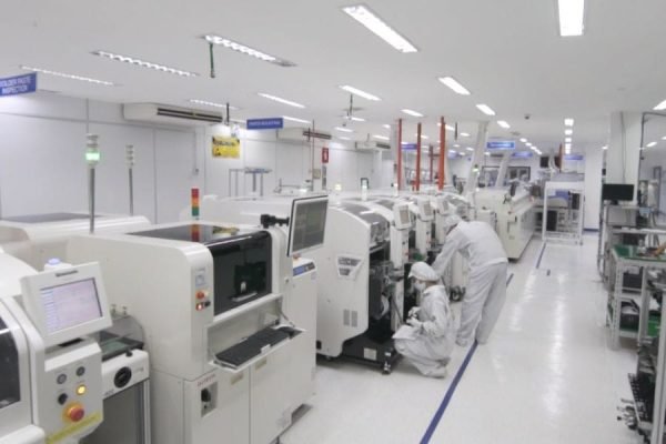
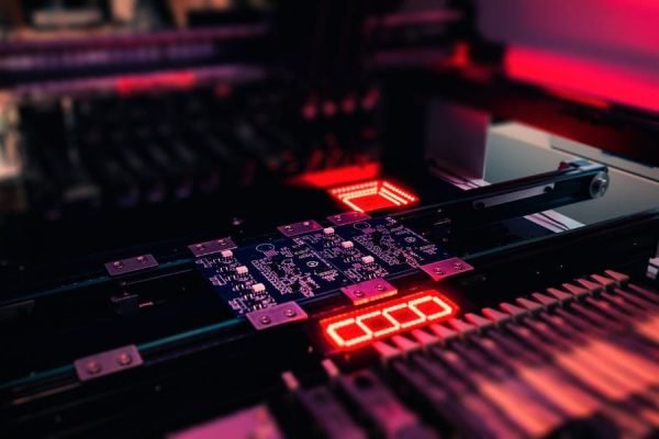
3. SMT Component Placement
— Pick-and-place machines mount components from 0201 chips to fine-pitch 0.4mm ICs with vision alignment. Dynamic bend zones remain strictly component-free. -
4. Controlled Reflow Soldering
— Panels pass through nitrogen reflow with profiles adapted to polyimide substrates (260°C capable, SAC305 or Sn63Pb37). The carrier prevents wrinkling, warpage, and pad shifting during heating. -
5. THT & Selective Soldering
— Through-hole parts, connectors, and ZIF contacts are inserted and soldered via selective soldering or precision hand soldering. Gold fingers receive protective handling. -
6. Inspection & Testing
— 100% AOI on all solder joints, X-ray for hidden joints (QFN/BGA on stiffened zones), electrical continuity testing, and final visual check of bend zones under magnification.
Why Flex Circuits Need Carrier Fixturing for Assembly
Flexible circuits cannot run through SMT lines unsupported — they wrinkle, sag, and shift during printing and reflow, destroying pad alignment. Assembly carriers made of aluminum or carbon fiber hold flex panels flat, maintain accurate printing height, and prevent thermal distortion in the reflow oven. Without carriers, first-pass yield drops sharply.
- 1. Carrier Materials — Aluminum (cost-effective, excellent heat distribution), carbon fiber (lightweight, dimensionally stable), and FR4 carriers for simpler jobs. All rated for 260°C reflow temperatures.
- 2. Fixturing Methods — High-temperature tape for low-volume runs, magnetic clamping for production panels, and vacuum fixturing for double-sided assembly passes.
- 3. Carrier Removal & Cleaning — After reflow and inspection, flex circuits are released from carriers, cleaned of adhesive residue, and returned to free-film form for final test and shipment.
DFM tip: Design flex panels with rigid rails or carrier tooling holes when possible. Panel-level delivery lets us run your circuits through standard SMT lines — the most cost-effective flex assembly method.
Stiffeners and Coverlay: Flex-Specific Requirements
Two flex-specific structures — stiffeners and coverlay — determine where components can be placed and how the circuit survives bending. We apply both in-house.
Stiffener Materials We Apply
| Stiffener Material | Thickness Range | Applied Where |
|---|---|---|
| Polyimide (PI) | 125–500µm | Local support under SMT pads; ZIF connector areas (0.2–0.3mm typical) |
| FR4 | 0.2–1.6mm | Rigid islands for THT components and heavy connectors |
| Stainless Steel | 0.1–0.5mm | High-strength zones; heat spreading for power devices |
| Aluminum | 0.5–2.0mm | Heat dissipation zones for LED and power components |
Coverlay Application Rules
- Coverlay Replaces Solder Mask — Adhesive-backed polyimide film protects traces on every bending zone. Liquid solder mask would crack during flexing.
- Pad Openings — Coverlay windows are cut ≥0.1mm larger than pads on each side, holding adhesive squeeze-out below 50% of pad width to prevent solder bridging paths.
- Bend Zone Construction — Copper sits at the neutral axis with coverlay on both sides for maximum flex fatigue life.
- ZIF Finger Exposure — Gold fingers for ZIF insertion are masked to tight thickness tolerance (0.3mm ±0.05 total stackup).
Flex PCB Assembly Capabilities
Our flexible circuit assembly line supports the following technical specifications:
| Parameter | Specification |
|---|---|
| Circuit Types | Single-sided, double-sided, multilayer flex, rigid-flex |
| Base Material | Polyimide (PI) 12.5–100µm (PET for non-reflow applications only) |
| Copper Foil | RA (rolled-annealed) / ED (electrodeposited), 1/3 oz – 2 oz |
| Minimum Component Size | 0201 (0603 metric) |
| Minimum IC Pitch | 0.4mm (on stiffened zones) |
| Assembly Types | SMT, THT, mixed technology, selective & hand soldering |
| Stiffeners | PI / FR4 / stainless steel / aluminum |
| Surface Finish | ENIG (recommended), OSP, immersion tin, immersion silver |
| Solder Alloys | SAC305 (lead-free), Sn63Pb37 (tin-lead) |
| Reflow Capability | Nitrogen reflow, profiles adapted for polyimide (260°C) |
| Inspection | 100% AOI, X-ray (QFN/BGA), electrical continuity test |
| MOQ | 1 piece (prototype) |
| Lead Time | 5–7 working days (prototype), 2–4 weeks (production) |
| Certifications | ISO 9001:2015, IATF 16949:2016 |
Flex vs Rigid PCB Assembly: Key Differences
Flexible and rigid circuit assemblies differ in support requirements, protective layers, and handling — not in soldering fundamentals:
| Aspect | Flex PCB Assembly | Rigid PCB Assembly |
|---|---|---|
| Substrate | Polyimide film, 12.5–100µm | FR4 / high-Tg laminate |
| Panel Support | Carrier fixturing mandatory | Panel rails sufficient |
| Protective Layer | Coverlay (adhesive-bonded PI film) | Liquid photoimageable solder mask |
| Component Areas | Stiffener-reinforced zones only | Entire board surface |
| Reflow | Adapted profiles, carrier-supported | Standard profiles |
| Bend Zones | No components, no vias allowed | Not applicable |
| Common Connectors | ZIF, crimped flex jumpers | Headers, board-to-board |
| Handling | ESD + crease protection | Standard ESD |
| Typical Use | Wearables, medical, camera modules | Most electronic products |
The soldering processes are identical — SMT, THT, and mixed technology with SAC305 or Sn63Pb37 alloys. What changes is everything around the soldering: carriers replace panel rigidity, coverlay replaces solder mask, and stiffeners create local mounting surfaces. Cost-wise, flex assembly carries a premium from carriers and handling, justified where 3D packaging, weight reduction, or dynamic motion is required.
Quality Standards and Certifications
IPC-A-610 Class 2/3
Solder joint acceptance criteria for flex assemblies. Class 3 available for medical, automotive, and aerospace applications.
IPC-6013
Performance qualification standard for flexible printed circuits — covering coverlay adhesion, copper wrap, and bend endurance.
IPC-2223
Flex circuit design standard we reference in DFM review — bend radius rules, stiffener placement, and bend-zone construction.
ISO 9001:2015
Certified quality management system covering all flex assembly processes from incoming inspection to shipment.
IATF 16949:2016
Automotive quality management for flex circuits in camera modules, sensors, and battery management systems.
RoHS & REACH
Full compliance with lead-free SAC305 as standard; tin-lead available for exempt applications.
Industries We Serve with Flex PCB Assembly
Wearables & Consumer
Smartwatch straps, TWS earbud batteries, folding phone hinge circuits, and camera module interconnects requiring ultra-thin stackups.
Medical Devices
Catheter sensors, hearing aids, wearable monitoring patches, and endoscope modules requiring Class 3 solder joints and full traceability.
Automotive
Camera modules, instrument clusters, EV battery management flex, and LiDAR interconnects built to IATF 16949.
Aerospace & Defense
Satellite harnesses, avionics interconnects, and weight-critical systems replacing bulky wiring looms with rigid-flex.
Industrial Automation
Robotic arms, dynamic sensor links, and machine vision cables surviving millions of flex cycles with RA copper construction.
IoT & Communications
Antenna modules, 5G device interconnects, and compact sensor nodes where 3D folding saves enclosure volume.
Frequently Asked Questions About Flex PCB Assembly
Flex PCB assembly is the process of mounting electronic components onto flexible printed circuits built from polyimide film. Components are attached using standard SMT and through-hole processes adapted for flexible substrates — with high-temperature carriers for panel support, stiffeners beneath component zones, and coverlay in place of solder mask.
Yes. SMDs from 0201 chips to fine-pitch 0.4mm ICs are routinely assembled on flex circuits, provided component areas sit on stiffened zones (PI or FR4) and panels run on rigid carriers through printing and reflow. Dynamic bend zones must remain component-free to prevent copper trace fatigue cracking.
Flexible circuits use polyimide (PI) base film from 12.5 to 100µm with RA (rolled-annealed) or ED copper foil in 1/3 to 2 oz weights. PET film is limited to non-reflow applications because it softens near 150°C. Stiffener options include PI, FR4, stainless steel, and aluminum; ENIG is the recommended surface finish for solderability and flatness.
Stiffeners are required wherever mechanical support is needed: under SMT pads for stable soldering, at ZIF connector insertion areas (typically 0.2–0.3mm PI or FR4 to meet thickness tolerance), and beneath THT components and heavy connectors. Without stiffeners, flexible areas deform during soldering and connector insertion cycles.
Coverlay is an adhesive-backed polyimide film that protects flex circuit traces where liquid solder mask would crack during bending. It replaces solder mask on all flexible zones, with openings cut for pads. Rigid sections of rigid-flex boards can use standard liquid solder mask, but every bending zone requires coverlay.
Yes. Rigid-flex assembly combines rigid islands for component mounting with flex sections for 3D interconnection — eliminating connectors and harnesses. We assemble rigid-flex boards with layer counts up to 20, soldering components on rigid areas while protecting flex sections during handling, and inspection includes bend-zone microscopy.
ZIF (zero insertion force) connectors are the most common flex termination — the flex tail inserts directly, with gold fingers at a controlled total thickness (typically 0.3mm ±0.05). Other options include crimped flex jumpers, board-to-board connectors mounted on stiffened zones, and direct soldering of flex tails to pads.
MOQ is 1 piece for prototypes. Standard flex assembly lead time is 5–7 working days for prototypes and 2–4 weeks for production volumes, including carrier preparation, SMT/THT assembly, 100% AOI, X-ray where required, and electrical testing. Send Gerber files, BOM, and flex drawings for a quote within 24 hours.
Ready to Start Your Flex PCB Assembly Project?
Send us your Gerber files, BOM, and flex circuit drawings. Our engineering team reviews bend zones, stiffener placement, and component layout, then provides a detailed quote within 24 hours.