BGA Assembly Services
Professional ball grid array PCB assembly with 100% X-ray inspection, precision reflow soldering, and expert BGA rework capability. From 0.4mm fine-pitch to 1.27mm standard-pitch BGA packages.
What Is BGA Assembly?
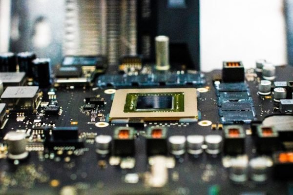
BGA (Ball Grid Array) assembly is the process of mounting integrated circuit packages with solder ball arrays onto a printed circuit board using surface mount technology. Unlike leaded packages such as QFP, BGA components connect through a grid of solder balls on the package underside, requiring X-ray inspection since the joints are hidden beneath the component body.
BGA packages are chosen for high-pin-count applications because they offer higher I/O density, shorter electrical paths, and better thermal dissipation than perimeter-leaded packages. Common applications include processors, FPGAs, memory chips, and networking ASICs.

BGA Package Types We Handle
JHYPCB handles the full range of BGA package types, from standard-pitch plastic BGAs to ultra-fine-pitch chip-scale packages.
| Package Type | Abbreviation | Pitch Range | Substrate | Typical Applications |
|---|---|---|---|---|
| Plastic BGA | PBGA | 1.0–1.27mm | BT resin | Microcontrollers, memory modules, consumer electronics |
| Ceramic BGA | CBGA | 1.0–1.27mm | Ceramic | Aerospace, military, high-reliability systems |
| Tape BGA | TBGA | 1.0–1.27mm | Polyimide tape | Telecommunications, servers, networking |
| Fine-Pitch BGA | FBGA | 0.5–0.8mm | Molded compound | Mobile devices, computing, storage |
| Chip Scale Package | CSP / WLCSP | 0.4–0.5mm | Various | Smartphones, wearables, IoT devices |
| Micro BGA | μBGA | 0.3–0.4mm | Various | Miniaturized sensors, medical devices |
Don’t see your package type? Contact us with your BGA datasheet — we evaluate every package on a case-by-case basis.
Our BGA Assembly Process
Every BGA assembly follows a controlled six-step process designed to maximize first-pass yield and ensure joint reliability per IPC-A-610 standards.
- 1. Stencil Printing — Solder paste is applied to PCB pads using precision stencils with apertures sized for BGA pitch. 3D SPI (Solder Paste Inspection) verifies paste volume on every BGA pad before placement.
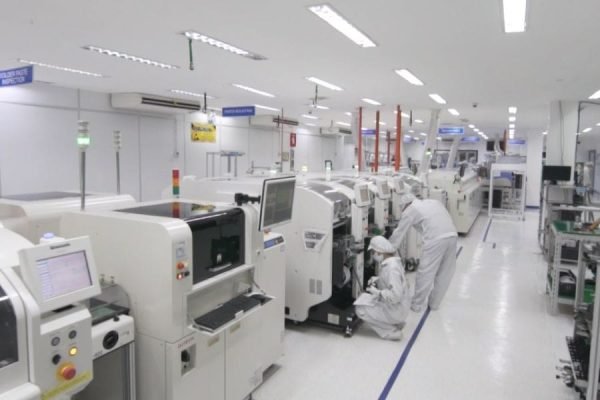
- 2. Precision Placement — BGA components are placed using automated pick-and-place machines with vision alignment. Placement accuracy is within microns to ensure each solder ball aligns with its corresponding pad.
- 3. Controlled Reflow Soldering — The board passes through a reflow oven with a thermal profile calibrated to the BGA package, solder alloy (SAC305 or Sn63Pb37), and PCB material. The profile includes preheat, soak, reflow, and cooling stages.
- 4. Post-Reflow AOI — Automated Optical Inspection checks component placement, polarity, and visible solder quality on surrounding non-BGA components.
- 5. X-Ray Inspection — 100% of BGA joints are inspected by X-ray to detect hidden defects: voids, bridges, misalignment, cold joints, and head-in-pillow (HIP).
- 7. Functional Testing — Electrical and functional testing verifies board performance and long-term reliability before shipment.
Why X-Ray Inspection Is Mandatory for BGA Assembly
BGA solder joints are completely hidden beneath the package body and cannot be inspected by visual or AOI methods. X-ray inspection is the only non-destructive technique capable of evaluating BGA joint quality, detecting voids, bridging, misalignment, cold joints, and head-in-pillow defects.
BGA Void Acceptance Criteria
| Standard Class | Application | Max Individual Void | Max Total Voiding |
|---|---|---|---|
| IPC-A-610 Class 2 | General electronics | ≤25% of joint area | ≤40% of pad area |
| IPC-A-610 Class 3 | High-reliability (aerospace, medical, automotive) | ≤10% of joint area | ≤25% of pad area |
| Customer-specific (automotive) | Safety-critical components | ≤15% per OEM spec | Per OEM spec |
JHYPCB performs 100% X-ray inspection on every BGA assembly. 2D X-ray for production screening; 3D CT available for first-article inspection and failure analysis.
What X-Ray Detects
- Voids — Gas pockets in solder joints; measured as percentage of pad area
- Bridging — Solder connecting adjacent balls
- Misalignment — BGA shifted from pad position
- Cold joints / Non-wet opens — Solder ball and paste did not coalesce
- Head-in-Pillow (HIP) — Ball and paste touched but did not bond; requires angled X-ray (45–70°) to detect
BGA Rework and Reballing Services
BGA components can be safely removed, reballed, and reassembled using specialized rework equipment. JHYPCB provides BGA rework services for prototyping, field returns, and design iteration — with full X-ray validation after every rework cycle.
- 1. Component Removal — Controlled heating with bottom preheat and top hot-air nozzle; vacuum pickup removes the BGA without damaging pads or surrounding components.
- 2. Site Preparation — Residual solder is cleaned from PCB pads using solder wick and specialized cleaning agents. Pads are inspected under magnification for damage.
- 3. Reballing — New solder balls are placed on the BGA package using a reballing stencil, then reflowed to attach. SAC305 lead-free or Sn63Pb37 tin-lead balls available.
- 4. Reassembly — Flux or solder paste is applied to PCB pads; the reballed BGA is aligned and reflowed using the original thermal profile.
- 5. Post-Rework X-Ray — Full X-ray inspection verifies joint quality after rework, ensuring reliability equivalent to first-pass assembly.
BGA Assembly Capabilities
Our BGA assembly line supports the following technical specifications:
| Parameter | Specification |
|---|---|
| Minimum BGA Pitch | 0.4mm (0.3mm for CSP with HDI) |
| Maximum Package Size | 50mm × 50mm |
| Maximum Ball Count | 3,000+ balls |
| Package Types | PBGA, CBGA, TBGA, FBGA, CSP, μBGA, LGA |
| Solder Alloys | SAC305 (lead-free), Sn63Pb37 (tin-lead) |
| Surface Finish Compatibility | ENIG, HASL, OSP, Immersion Silver, Immersion Tin |
| X-Ray Inspection | 100% BGA joints (2D standard, 3D CT available) |
| Reflow Atmosphere | Air or Nitrogen (N₂) |
| MOQ | 1 piece (prototype) |
| Lead Time | 3–5 days (prototype), 2–4 weeks (production) |
| Certifications | ISO 9001:2015, IATF 16949:2016 |
BGA vs QFP vs LGA Package Comparison
When selecting IC packages for high-density PCB designs, engineers compare BGA, QFP, and LGA across several criteria:
| Feature | BGA | QFP | LGA |
|---|---|---|---|
| Connection Method | Solder ball grid | Perimeter leads | Flat pad grid |
| Pitch Range | 0.4–1.27mm | 0.4–0.8mm | 0.5–1.0mm |
| I/O Density | Highest (full area array) | Medium (perimeter only) | High (full area array) |
| Thermal Performance | Excellent (direct path) | Limited (through leads) | Excellent (direct path) |
| Electrical Performance | Low inductance, short paths | Higher inductance, longer paths | Low inductance |
| Self-Alignment | Yes (surface tension) | Limited | Yes (surface tension) |
| Inspection Method | X-ray required | Visual / AOI possible | X-ray recommended |
| Rework Difficulty | Moderate | High (lead damage risk) | Moderate |
| Typical Applications | CPUs, GPUs, FPGAs, memory | MCUs, ASICs, industrial ICs | CPUs (Intel), server chips |
BGA offers the highest I/O density and best electrical performance but requires X-ray inspection. QFP is easier to inspect visually but is limited in pin count and thermal performance. LGA combines BGA’s density advantages with flat-pad connections, often used in socket-mounted CPU applications.
Quality Standards & Certifications
IPC-A-610 Class 2/3
BGA solder joints inspected to IPC-A-610 acceptance criteria. Class 3 available for high-reliability applications including aerospace, medical, and automotive safety.
IPC-7095
BGA design and assembly process implementation per IPC-7095 standard, covering void management, rework procedures, and reliability guidelines.
J-STD-001
Soldering requirements per J-STD-001 joint standard, ensuring metallurgical bond quality and intermetallic compound formation.
ISO 9001:2015
Quality management system certified to ISO 9001:2015, covering all PCB assembly processes from incoming inspection to final shipment.
IATF 16949:2016
BGA design and assembly process implementation per IPC-7095 standard, covering void management, rework procedures, and reliability guidelines.
RoHS & REACH
All BGA assemblies comply with RoHS and REACH directives. Lead-free SAC305 solder standard; tin-lead available for exempt applications.
Industries We Serve with BGA Assembly
Automotive
ADAS modules, engine ECUs, infotainment systems, and battery management controllers requiring IATF 16949 compliance and Class 3 reliability.
Telecommunications
Networking ASICs, baseband processors, and 5G infrastructure modules requiring high I/O density and thermal management.
Medical Devices
Diagnostic equipment, patient monitoring, and imaging systems requiring Class 3 solder joints and full traceability.
Aerospace & Defense
Avionics, satellite communication, and mission-critical systems requiring hermetic CBGA packages and zero-defect acceptance.
Consumer Electronics
Processors, GPUs, memory modules, and gaming consoles requiring cost-effective high-volume BGA assembly.
Industrial Controls
PLC controllers, motor drives, and industrial IoT gateways requiring long-term reliability in harsh environments.
Frequently Asked Questions About BGA Assembly
BGA assembly is the process of mounting ball grid array integrated circuit packages onto a printed circuit board using surface mount technology. BGA components connect through a grid of solder balls on the package underside, which melt during reflow soldering to form electrical and mechanical joints. X-ray inspection is required because the joints are hidden beneath the component.
BGA solder joints are located beneath the package body and cannot be seen by visual inspection or AOI. X-ray is the only non-destructive method to detect hidden defects including voids, bridging, misalignment, cold joints, and head-in-pillow (HIP). IPC-A-610 and IPC-7095 require X-ray verification for BGA joint acceptance.
JHYPCB assembles BGA packages with pitch as fine as 0.4mm (0.3mm for chip-scale packages with HDI PCB technology). Fine-pitch BGA assembly requires ultra-fine stencil apertures, precision pick-and-place with vision alignment, and controlled nitrogen reflow to prevent bridging and voiding.
Yes. We provide BGA rework services including component removal, pad cleaning, reballing, and reassembly using specialized rework stations with bottom preheating and vacuum pickup. Every reworked BGA undergoes full X-ray inspection to verify joint reliability equivalent to first-pass assembly.
Per IPC-A-610, Class 2 (general electronics) allows individual voids up to 25% of joint area. Class 3 (high-reliability: aerospace, medical, automotive) limits individual voids to 10% with total voiding below 25%. Customer-specific requirements for automotive safety components may specify ≤15%.
We assemble all major BGA package types including PBGA (plastic), CBGA (ceramic), TBGA (tape), FBGA (fine-pitch), CSP (chip-scale), and micro BGA (μBGA). We also support LGA (land grid array) packages. Package pitch ranges from 0.4mm to 1.27mm with ball counts up to 3,000+.
Ready to Start Your BGA Assembly Project?
Send us your Gerber files, BOM, and BGA datasheets. Our engineering team will review your design and provide a detailed quote within 24 hours.