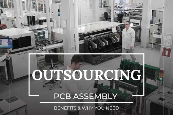
Lead-Free PCB Assembly Service
RoHS and REACH compliant PCB assembly using SAC305, SAC307, and SN100C lead-free solder alloys. Fully certified for global electronics markets.
oHS ✓ · REACH ✓ · IPC-A-610 ✓ · UL Listed ✓
Lead-Free Solder Alloys We Use
We select lead-free solder alloys based on your application requirements — balancing cost, wetting performance, joint reliability, and thermal cycling resistance. All alloys below comply with RoHS 3 (Directive 2015/863) and REACH regulations.
| Alloy | Composition | Melting Range | Key Properties | Typical Application |
|---|---|---|---|---|
| SAC305 | Sn96.5 / Ag3.0 / Cu0.5 | 217–220°C | Industry standard, excellent wetting, good thermal fatigue | General SMT reflow, most common lead-free alloy |
| SAC307 | Sn99.0 / Ag0.3 / Cu0.7 | 217–227°C | Lower silver content reduces cost, acceptable for non-critical joints | Cost-sensitive consumer electronics |
| SN100C | Sn99.25 / Ag0.25 / Cu0.5 / Ni0.05 + Ge | 227°C | Flat bright joints, excellent fluidity, reduced copper dissolution | Wave soldering, THT assembly |
| SnAg3.5 | Sn96.5 / Ag3.5 | 221°C | High reliability, superior thermal fatigue resistance | Automotive, industrial, harsh-environment electronics |
| SnCu0.7 (N₂) | Sn99.3 / Cu0.7 | 227°C | Lowest cost lead-free wave soldering alloy, requires nitrogen atmosphere | High-volume wave soldering for THT |
SAC305 remains our default for SMT reflow applications due to its proven reliability and broad industry acceptance. For through-hole wave soldering, SN100C is preferred for its superior fluidity and reduced copper pad dissolution.
Lead-Free Compatible Surface Finishes
The PCB surface finish you choose directly affects lead-free solder joint quality, shelf life, and cost. Not all finishes perform equally with SAC305 and other lead-free alloys. The table below helps you select the right finish for your lead-free project.
| Surface Finish | Shelf Life | Solderability | Flatness | Cost | Best For |
|---|---|---|---|---|---|
| ENIG | 12+ months | Excellent | Excellent (flat) | High | BGA, QFN, fine-pitch SMT — best overall choice for lead-free |
| OSP | 3–6 months | Good (first reflow only) | Good | Low | Cost-sensitive single-side SMT boards — not suitable for double-sided or wave soldering |
| HASL Lead-Free | 12+ months | Good | Poor (uneven) | Low | THT and mixed-technology boards — avoid for fine-pitch BGA |
| Immersion Silver | 6–12 months | Very Good | Excellent | Medium | High-frequency/RF boards, fine-pitch SMT — requires anti-tarnish packaging |
| Immersion Tin | 6–12 months | Good | Excellent | Medium | Press-fit connectors, fine-pitch SMT — tin whisker risk, evaluate for reliability-critical use |
RoHS & REACH Compliance
Every lead-free assembly project we deliver comes with full compliance documentation. We maintain material declarations and third-party test reports for all solder materials, fluxes, and surface finishes used in production.
- RoHS 3 Compliance (2015/863): All solder alloys, fluxes, and surface finishes (HASL lead-free, ENIG, OSP) comply with the latest RoHS 3 directive, restricting 10 substances including lead (Pb), mercury, cadmium, and phthalates.
- REACH Compliance (EC 1907/2006): We provide SVHC (Substances of Very High Concern) declarations for all materials. No substances on the current REACH SVHC candidate list are intentionally added to our solder pastes or fluxes.
- Conflict Minerals (Dodd-Frank §1502): Tin, tungsten, tantalum, and gold in our solder materials are sourced from conflict-free smelters certified under the RMI (Responsible Minerals Initiative) program.
| Document | Content | Provided With |
|---|---|---|
| Material Declaration (MD) | Full composition of solder alloys, fluxes, finishes | Every production order |
| RoHS Compliance Certificate | Declaration of conformity to RoHS 3 | On request |
| REACH SVHC Declaration | Statement of SVHC content per candidate list | On request |
| Third-Party Test Report | SGS or Intertek XRF testing results | On request |
| IPC Certificate of Conformity | J-STD-001 compliance statement | Every production order |
Lead-Free Reflow Soldering Profile
Lead-free reflow requires higher peak temperatures than tin-lead soldering — typically 240–260°C versus 210–230°C. Our reflow profiles are engineered per JEDEC J-STD-020 and IPC-7530 standards to ensure proper wetting while minimizing thermal stress on components and laminate.
| Zone | Temperature Range | Dwell Time | Purpose |
|---|---|---|---|
| Preheat (Zone 1–3) | 25 → 150°C | 60–90 sec | Evaporate solvent from flux; activate flux chemistry; prevent thermal shock to components |
| Soak / Thermal Stabilization (Zone 4–5) | 150 → 200°C | 60–120 sec | Uniform board temperature; activate flux; reduce ΔT across PCB to prevent tombstoning |
| Reflow Peak (Zone 6–7) | 240 – 260°C (peak) | 30–60 sec above 217°C (liquidus) | Melt solder alloy; form metallurgical bond; ensure proper wetting and fillet formation |
| Cooling (Zone 8) | 260 → 70°C | 60–90 sec (4–6°C/sec cooling rate) | Solidify solder joints; controlled cooling prevents grain coarsening and improves joint reliability |
Lead-Free vs Leaded Assembly: Key Differences
Understanding the differences between lead-free and traditional tin-lead assembly helps you make informed decisions for your project. The table below summarizes the critical technical and commercial differences.
| Parameter | Lead-Free (SAC305) | Leaded (Sn63Pb37) | Impact |
|---|---|---|---|
| Melting Point | 217–220°C | 183°C | Lead-free requires +30–40°C higher reflow temps |
| Reflow Peak | 240–260°C | 210–230°C | Components must rated for 260°C lead-free profile |
| Wetting | Slower wetting, duller appearance | Fast wetting, bright shiny joints | Lead-free joints appear different but are equally reliable when properly formed |
| Surface Finish Compatibility | ENIG, OSP, HASL lead-free, Imm Silver, Imm Tin | HASL tin-lead | Lead-free requires compatible surface finishes |
| Thermal Fatigue | Better in thermal cycling | Better in vibration/mechanical stress | Application-dependent — lead-free preferred for thermal cycling, leaded for mechanical stress |
| Cost | +15–30% (higher silver content, higher temp equipment) | Lower | Lead-free carries a cost premium |
| RoHS/REACH | ✅ Compliant | ❌ Non-compliant (contains lead) | Lead-free required for EU, California, and most global markets |
| Rework Difficulty | Harder — higher melt temp, faster oxidation | Easier — lower melt temp, better wetting | Lead-free rework requires more skill and nitrogen assistance |
Our Lead-Free Assembly Capabilities
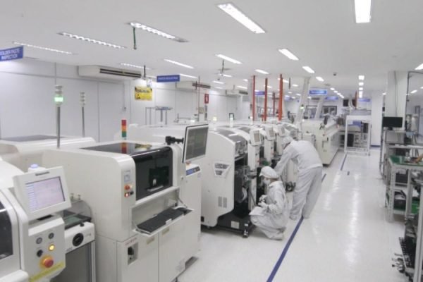
Our lead-free PCB assembly facility is equipped for both SMT and through-hole processes, supporting prototype to mid-volume production with full RoHS compliance at every stage.
PCB Specifications:
| Parameter | Capability |
|---|---|
| Max PCB Size | 535 × 840 mm |
| Layer Count | 1–32 layers |
| Board Thickness | 0.1–8.0 mm |
| Surface Finish | ENIG, OSP, HASL Lead-Free, Immersion Silver, Immersion Tin |
| Min Trace/Space | 2 / 2 mil |
| Min Hole Size | 0.15 mm (mechanical drill) |
Assembly Capability:
| Parameter | Capability |
|---|---|
| SMT Component Range | 01005 (0.4 × 0.2 mm) to 50 × 50 mm |
| THT Component Types | Axial, Radial, DIP, SIP, Custom |
| Placement Speed | Up to 36,000 CPH |
| Reflow Zones | 10-zone lead-free profile |
| Wave Soldering | Lead-free wave with N₂ atmosphere |
| Inspection | 100% AOI + X-ray (AXI) for BGA/QFN |
| Daily Capacity | Up to 5 million solder joints |
ISO 9001:2015
Quality management system certified for lead-free assembly processes
IATF 16949:2016
Automotive quality standard — lead-free assemblies for vehicle electronics
UL Listed
UL certification for lead-free PCB assemblies (E-number on file)
Lead-Free Solder Joint Quality Standards
Lead-free solder joints look different from tin-lead joints — they are typically duller and less shiny. This is normal and does not indicate a defect. We inspect all lead-free assemblies to IPC-A-610 Acceptability of Electronic Assemblies standards, with full documentation available.
- IPC-A-610 Class 2 & 3: All lead-free solder joints inspected to IPC-A-610. Class 2 (dedicated service electronics) is our default; Class 3 (high-reliability) is available for automotive, medical, and aerospace applications.
- J-STD-001 Soldering Requirements: Soldering processes and materials certified to J-STD-001, covering material requirements, process controls, and acceptance criteria for lead-free soldered connections.
- 100% AOI Inspection: Automated Optical Inspection (AOI) on every assembly, checking solder volume, fillet shape, bridging, tombstoning, and component placement for both SMT and THT joints.
- X-Ray Inspection (AXI): For BGA, QFN, and hidden-joint components, X-ray inspection verifies solder ball integrity, void percentage (<25% per IPC-7095), and complete wetting under hidden leads.
Industries & Applications Served
Lead-free PCB assembly is not one-size-fits-all. Different industries demand different reliability classes, traceability levels, and compliance documentation. We tailor our lead-free processes to meet your industry’s specific requirements.
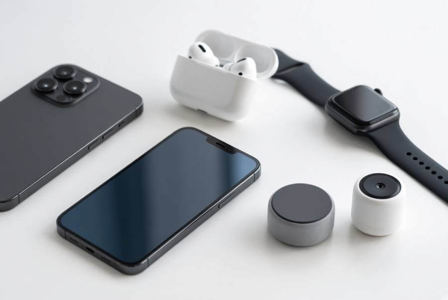
Consumer Electronics
High-volume, cost-optimized lead-free assembly to IPC-A-610 Class 2. Ideal for smart home devices, wearables, and IoT products targeting global markets.
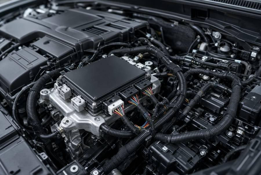
Automotive Electronics
IATF 16949 certified lead-free assembly to IPC-A-610 Class 3. Thermal cycling reliability, full material traceability, and PPAP documentation available for vehicle ECUs and sensor modules.
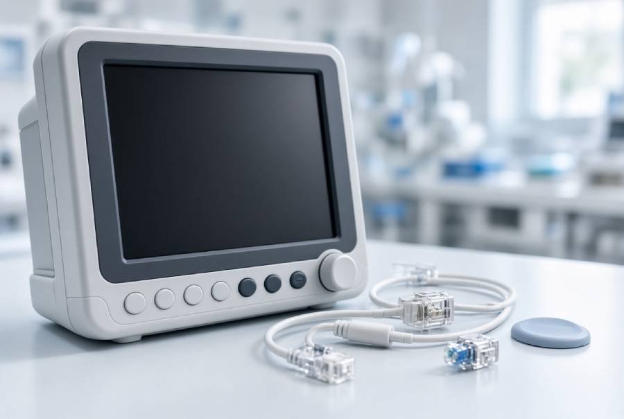
Medical Devices
ISO 9001 quality system with full traceability for lead-free medical PCBs. Cleanroom-compatible assembly, conformal coating, and documented processes for patient-connected and diagnostic equipment.
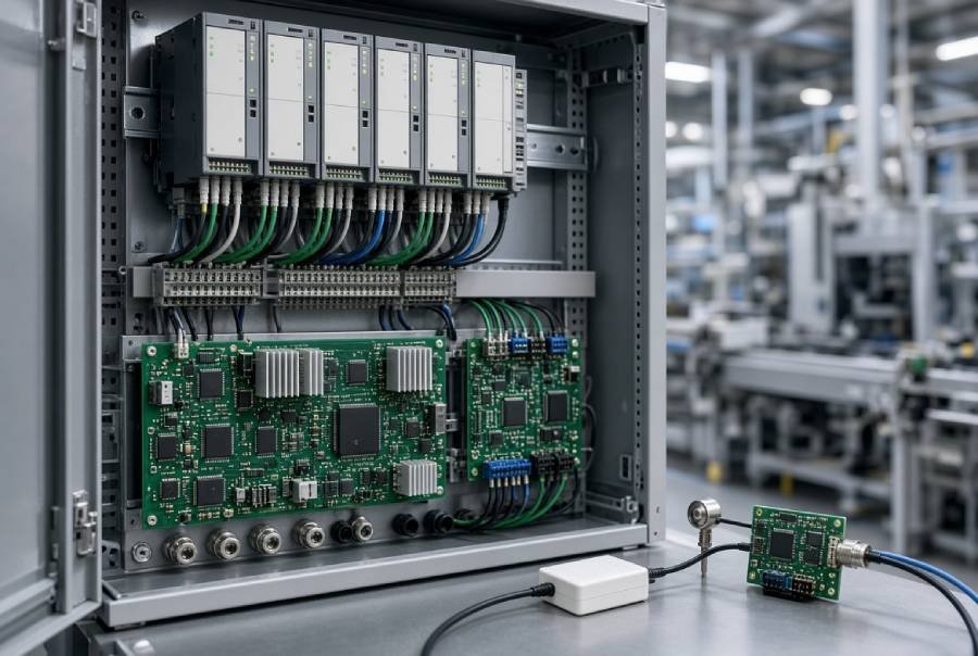
Industrial & IoT
Harsh-environment lead-free assembly for industrial control boards, power management modules, and connected sensors. Conformal coating and extended thermal cycling testing available.
Frequently Asked Questions
Lead-free PCB assembly is the process of soldering electronic components to a printed circuit board using solder alloys that contain no lead (Pb), typically tin-silver-copper (SAC) alloys. It is required for compliance with the EU RoHS Directive, which restricts hazardous substances including lead in electronic products.
We primarily use SAC305 (Sn96.5/Ag3.0/Cu0.5) for SMT reflow soldering and SN100C for through-hole wave soldering. Alternative alloys such as SAC307, SnAg3.5, and SnCu0.7 (nitrogen wave) are available for specific applications. We can also accommodate customer-specified alloys upon request.
Yes. All our lead-free solder alloys, fluxes, and surface finishes comply with RoHS 3 (Directive 2015/863) and REACH (EC 1907/2006). We provide material declarations, RoHS compliance certificates, REACH SVHC declarations, and third-party SGS/Intertek test reports with your production order.
Yes, but this requires a sequential process: lead-free reflow first (higher temperature), then leaded wave or hand soldering for specific through-hole components. This is sometimes used when certain components are not rated for 260°C lead-free reflow. We evaluate each mixed-alloy requirement case by case.
There is no strict minimum — we accept orders from a single prototype board to high-volume production. However, for very small quantities, a setup fee may apply. Contact us with your BOM and Gerber files for a detailed quote.
We inspect all lead-free assemblies to IPC-A-610 (Class 2 or 3) standards using 100% Automated Optical Inspection (AOI) for SMT joints and X-ray inspection (AXI) for BGA/QFN hidden joints. Lead-free solder joints naturally appear duller than tin-lead joints — this is normal and does not indicate a quality issue.